
Test socket and test apparatus having the same, manufacturing method for the test socket

a manufacturing method and test socket technology, applied in the field of test sockets, can solve the problems of inability to obtain desired impedance, inability to precisely control the stroke of the conventional test apparatus, inability to precisely control the stroke, etc., and achieve the effect of minimizing the loss of signal transmission and excellent high-frequency signal transmission characteristics

Active Publication Date: 2021-09-23
TSE CO LTD
View PDF0 Cites 0 Cited by
  • Summary
  • Abstract
  • Description
  • Claims
  • Application Information

AI Technical Summary

Benefits of technology

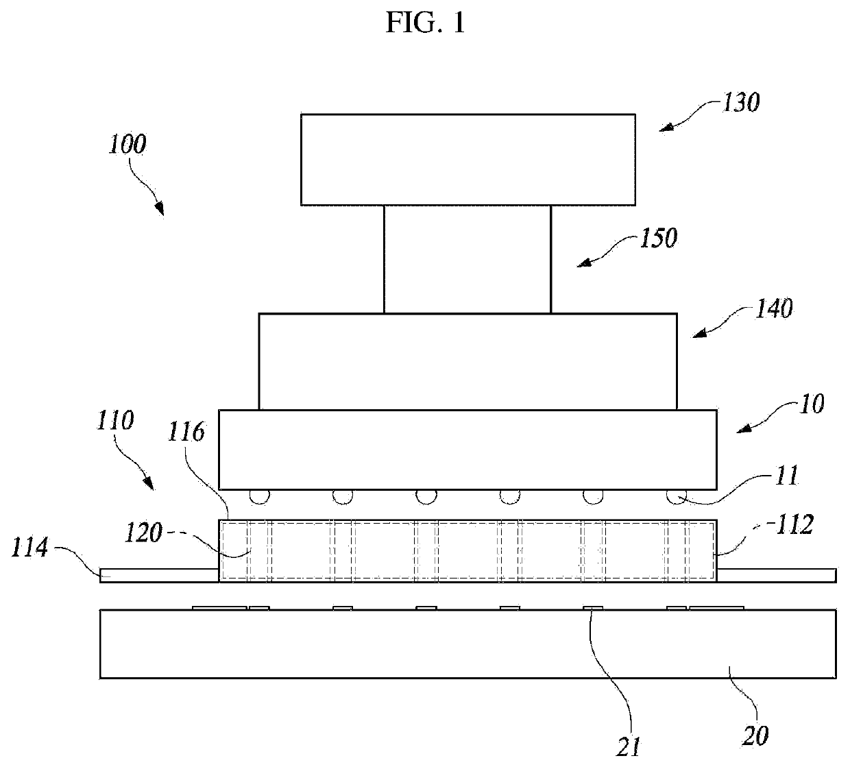
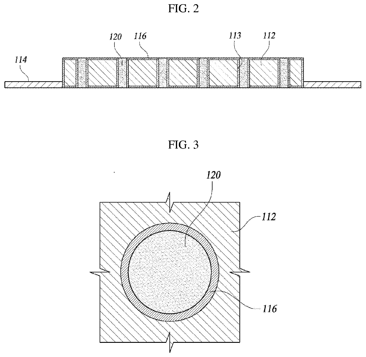
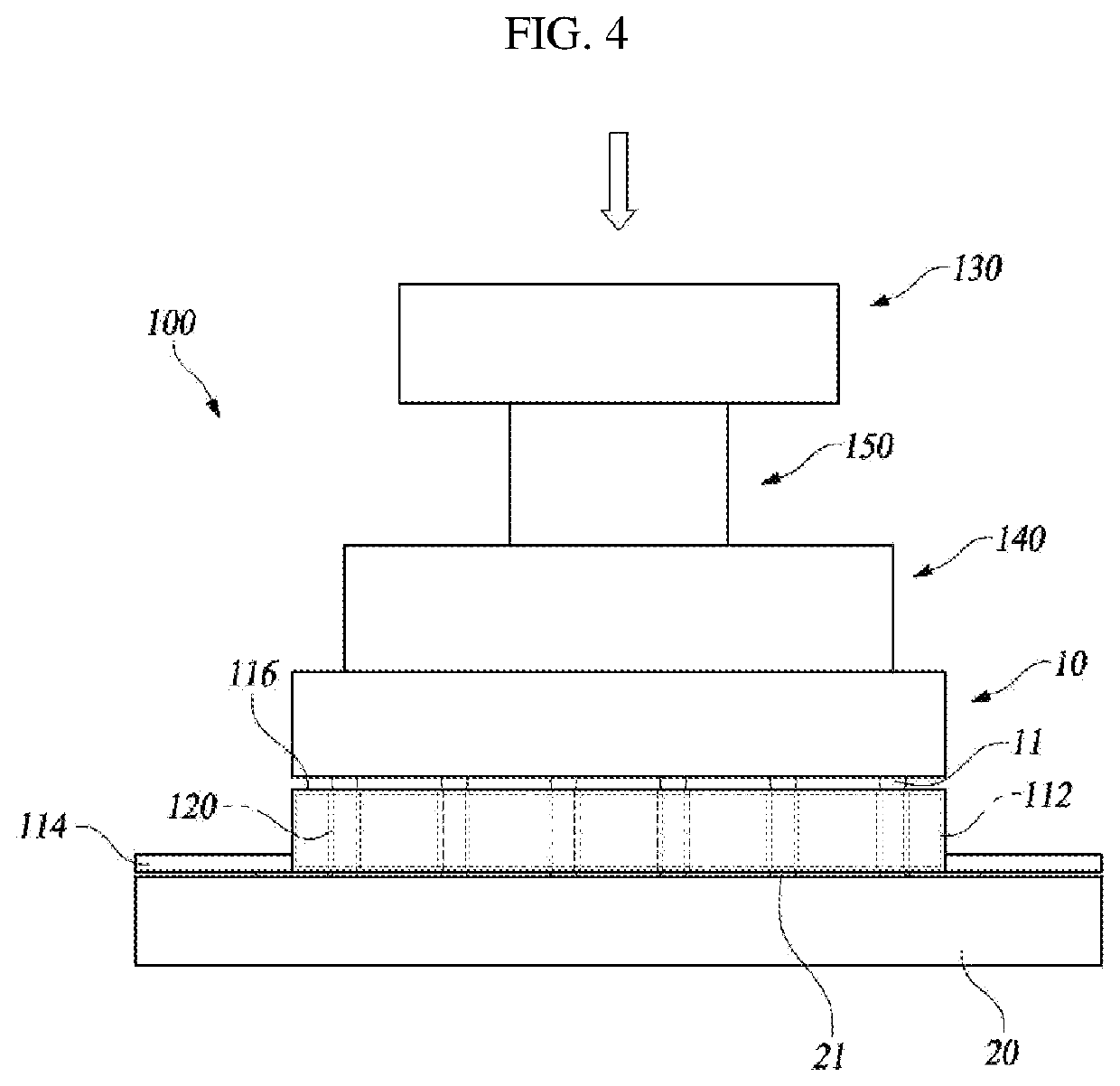
The present patent provides a test socket for controlling the stroking of a device under inspection with precision. The test socket includes a nonelastic electrically-conductive housing and a plurality of electrically-conductive parts. The nonelastic electrically-conductive housing ensures even distribution of pressure between the device under inspection and the tester, while the insulating part prevents signal interference and minimizes signal transmission loss. The test socket is also advantageous for high-speed signal transmission due to its matching of characteristic impedance.

Problems solved by technology

However, the conventional test apparatus had difficulty in precise stroke control due to an addition of a thickness tolerance of the stroke limiting part, a thickness tolerance of the stopper part, a height tolerance of the test socket, and a thickness tolerance of the semiconductor package.
In addition, the conventional rubber socket type test socket has problems in that since the insulating part is formed of a non-conductive material, high-frequency signal interference between the conductive parts could not be avoided, and a desired impedance could not be obtained, whereby high-frequency signal transmission characteristics is degraded.

Method used


Image

  • Test socket and test apparatus having the same, manufacturing method for the test socket
  • Test socket and test apparatus having the same, manufacturing method for the test socket
  • Test socket and test apparatus having the same, manufacturing method for the test socket

Examples


Embodiment Construction

[0052]The present invention now will be described more fully hereinafter with reference to the accompanying drawings, in which embodiments of the invention are shown. This invention may, however, be embodied in many different forms and should not be construed as limited to the embodiments set forth herein. Rather, these embodiments are provided so that this disclosure will be thorough and complete, and will fully convey the scope of the invention to those skilled in the art.

[0053]The terminology used herein is for the purpose of describing particular embodiments only and is not intended to be limiting of the invention. As used herein, the singular forms “a”, “an” and “the” are intended to include the plural forms as well, unless the context clearly indicates otherwise. It will be further understood that the terms “includes”, “comprises” and / or “comprising,” when used in this specification, specify the presence of stated features, integers, steps, operations, elements, and / or compone...


PUM

PropertyMeasurementUnit
electrically-conductiveaaaaaaaaaa
thicknessaaaaaaaaaa
nonelastic electrically-conductiveaaaaaaaaaa

Abstract

The present invention relates to a test socket configured to electrically connect a tester generating a test signal and a device under inspection to each other includes a nonelastic electrically-conductive housing having a plurality of housing holes passing therethrough in a thickness direction, an insulating coating layer applied on at least an upper surface of the nonelastic electrically-conductive housing and a circumference of each of the plurality of housing hole, and an electrically-conductive part formed to have a configuration in which a plurality of electrically-conductive particles are contained in an elastic insulating material, disposed in the housing hole such that a lower end portion thereof may be connected to a signal electrode of the tester placed below the nonelastic electrically-conductive housing.

Description

CROSS-REFERENCE TO RELATED APPLICATION[0001]This application claims priority of Korean Patent Application No. 10-2020-0033952, filed on Mar. 19, 2020, in the KIPO (Korean Intellectual Property Office), the disclosure of which is incorporated herein entirely by reference.BACKGROUND OF THE INVENTIONField of the Invention[0002]The present disclosure relates to a test socket, and more particularly, to a test socket configured to electrically connect a device under inspection and a tester to each other, a test apparatus including the same, and a method for manufacturing the test socket.Description of the Related Art[0003]A semiconductor package is formed by integrating fine electronic circuits at a high density, and during the manufacturing process, a test process is performed to determine whether each electronic circuit is normal. The test process is a process of selecting good and defective products by testing whether the semiconductor package is operating normally.[0004]A test apparat...

Claims


Application Information

Patent Timeline
Patent Type & Authority Applications(United States)
IPC IPC(8): G01R31/28G01R1/04
CPCG01R31/2889G01R1/0441G01R31/2896G01R31/2886G01R31/2601G01R1/0416G01R3/00G01R1/0433G01R1/0483G01R1/0466G01R1/07307
Inventor OH, CHANG SUKIM, BO HYUN
Owner TSE CO LTD
Learn More