Data processing system

a data processing system and transaction interface technology, applied in the field of data processing systems, can solve the problems of increasing the production quantity needed for a soc vendor to make a profit, the development cost of the soc, and the break-even level, so as to reduce power consumption and reduce the latency

Inactive Publication Date: 2009-03-05
RENESAS TECH CORP
View PDF10 Cites 13 Cited by
  • Summary
  • Abstract
  • Description
  • Claims
  • Application Information

AI Technical Summary

Benefits of technology

[0029](15) A data processing system includes: a first semiconductor integrated circuit;.and a second semiconductor integrated circuit, each of the first semiconductor integrated circuit and the second semiconductor integrated circuit possesses an initiator and a target to perform communication of encrypted information using a split transaction interface. The first semiconductor integrated circuit and the second semiconductor integrated circuit are coupled with a signal line for communication, and the first semiconductor integrated circuit changes a cryptographic key to be used in encryption after stopping the initiator of the second semiconductor integrated circuit. Accordingly, it becomes possible to change the cryptographic key, by suppressing the situation where the target of the first semiconductor integrated circuit becomes impossible to decrypt the request packet normally.
[0030](16) A data processing system includes: a first semiconductor integrated circuit; and a second semiconductor integrated circuit, each of the first semiconductor integrated circuit and the second semiconductor integrated circuit possesses an initiator and a target operable to perform communication using a split transaction interface. The first semiconduct...

Problems solved by technology

These tendencies raise the development costs of the SoC, such as a mask cost, through the synergistic effect.
Consequently, a mass production quantity necessary for a SoC vendor to make a profit, i.e., a break-even level, is abruptly going up in recent years.
However, employing parallel buses are often accompanied by some issues such as increased chip ...

Method used


Image

  • Data processing system
  • Data processing system
  • Data processing system

Examples


first embodiment

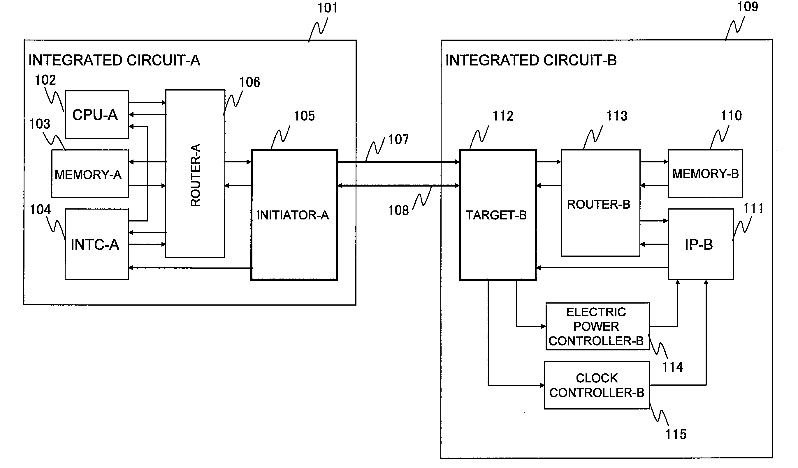
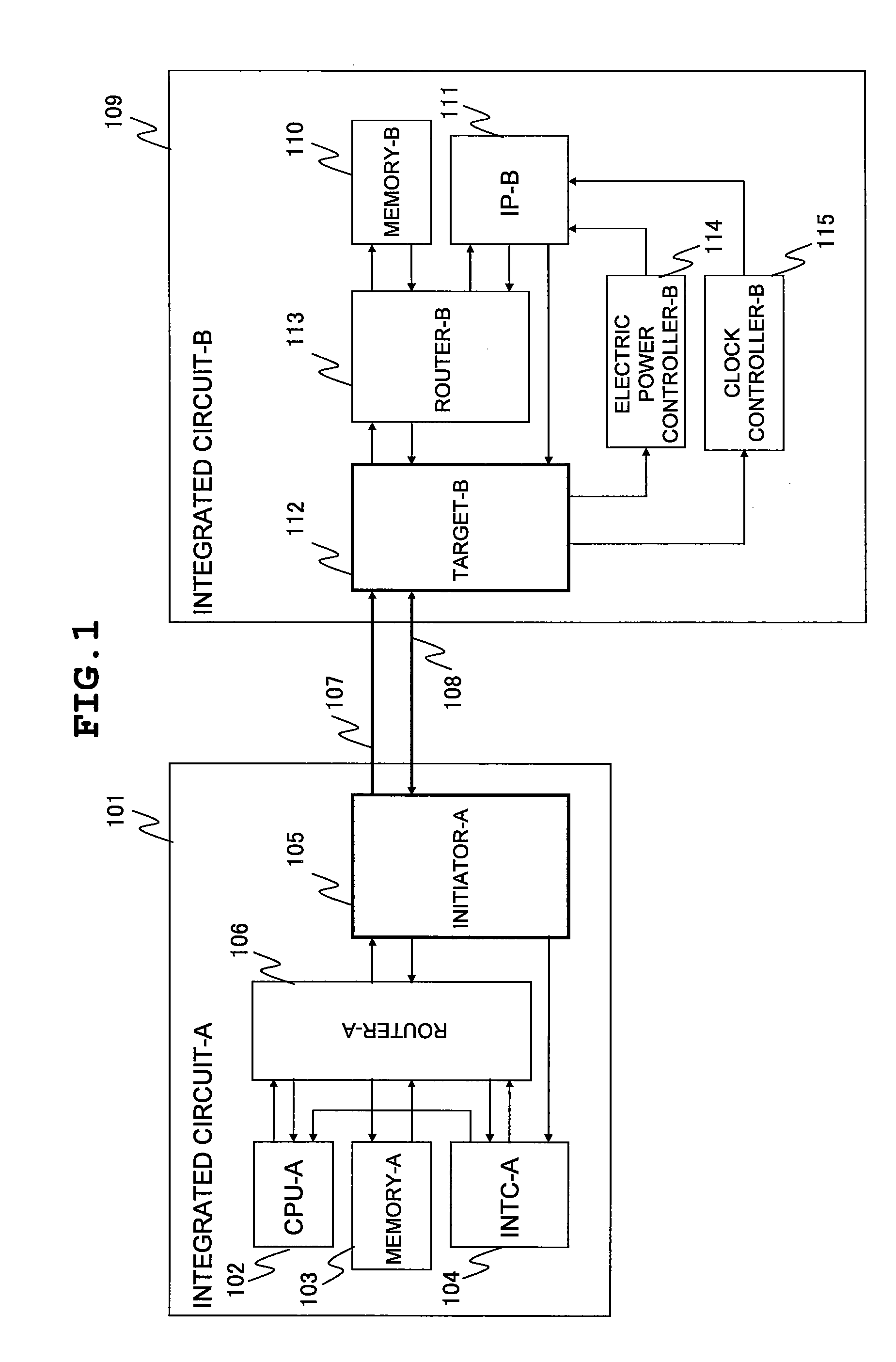
[0064]FIG. 1 illustrates an integrated circuit-A and an integrated circuit-B according to a first embodiment of the present invention. The integrated circuit-A 101 and the integrated circuit-B 109 illustrated in FIG. 1 are formed on a semiconductor substrate such as a single crystal silicon, employing semiconductor integrated circuit technology which forms a publicly known CMOS (complementary MOS transistor), a bipolar transistor, etc. The present embodiment explains the read access and the write access between the integrated circuit-A 101 and the integrated circuit-B 109 and the notice of interruption from the integrated circuit-B 109 to the integrated circuit-A 101.

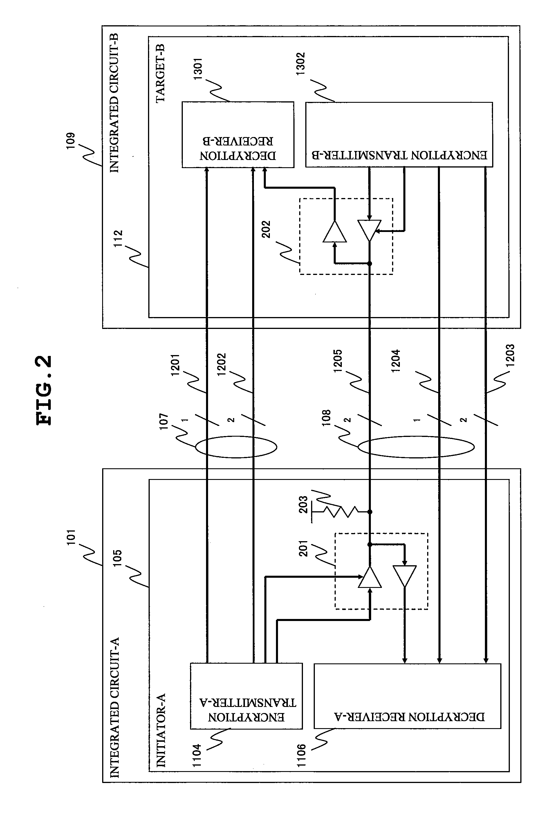
[0065]First, a signal line group-AB 107 and a signal line group-BA 108 are explained with reference to FIG. 2.

[0066]FIG. 2 is an arrangement chart illustrating the signal line group-AB 107 and signal line group-BA 108. Three-state buffers 201 and 202 switch a signal transmission direction. A pull-up resistor 203 fixes t...

second embodiment

[0287]Hereafter, a second embodiment of the present invention is described with reference to accompanying drawings.

[0288]FIG. 21 is a block diagram illustrating an integrated circuit-A and an integrated circuit-B according to another embodiment of the present invention. The integrated circuit-A 2101 and the integrated circuit-B 2111 illustrated in FIG. 21 are formed on a semiconductor substrate such as single crystal silicon, employing semiconductor integrated circuit technology which forms a publicly known CMOS (a complementary MOS transistor), a bipolar transistor, etc. The present embodiment explains read access, write access, and notice of interruption between the integrated circuit-A 2101 and the integrated circuit-B 2111 according to the second embodiment of the present invention, in case that both integrated circuits access mutually as an initiator.

[0289]A signal line group-AB 2121 transmits information from the integrated circuit-A 2101 to the integrated circuit-B 2111. A si...


PUM


Abstract

A data processing system enabling an outstanding-based variable flow control is provided. The data processing system includes a first semiconductor integrated circuit possessing an initiator and a second semiconductor integrated circuit possessing a target. The initiator transmits a request packet to the target, the target transmits a response packet to the initiator, and split transaction interface is practiced. The initiator includes an outstanding number counting circuit for counting an outstanding number defined by the difference in number between the request packets transmitted and the response packets received. The request packet transmission number is controlled so that the count value of the outstanding number counting circuit may not exceed the outstanding number to which the target can respond. The outstanding number is dynamically changeable to a suitable number so that the maximum latency from the issue of the request packet to the reception of the response packet is suppressed.

Description

CLAIM OF PRIORITY[0001]The Present application claims priority from Japanese patent application JP 2007-225030 filed on Aug. 31, 2007, the content of which is hereby incorporated by reference into this application.FIELD OF THE INVENTION[0002]The present invention relates to split transaction interface control in a data processing system in which plural semiconductor integrated circuits are coupled by a split transaction interface.BACKGROUND OF THE INVENTION[0003]Performance requirement and function requirement to a system-on-chip (SoC) are increasing every year, and the tendency is likely to continue. In connection with the tendency, the circuit quantity to be integrated on a SoC increases and miniaturization technique further advances to mount the increasing circuits on a chip. These tendencies raise the development costs of the SoC, such as a mask cost, through the synergistic effect. Consequently, a mass production quantity necessary for a SoC vendor to make a profit, i.e., a bre...

Claims


Application Information

Patent Timeline
IPC IPC(8): H04L12/56G06F13/38H04L29/08
CPCG06F13/4045Y02B60/1235Y02B60/1228Y02D10/00
Inventor NONOMURA, ITARU
Owner RENESAS TECH CORP
Why Eureka
Try Eureka