Method of manufacturing stacked semiconductor package using improved technique of forming through via

a semiconductor and packaging technology, applied in semiconductor devices, semiconductor/solid-state device details, electrical devices, etc., can solve the problems of waveform distortion and electrical crosstalk, signal loss increase, and the inability to completely fill the via hole,

Inactive Publication Date: 2010-02-25
ELECTRONICS & TELECOMM RES INST
View PDF8 Cites 6 Cited by
  • Summary
  • Abstract
  • Description
  • Claims
  • Application Information

AI Technical Summary

Benefits of technology

[0007]The present invention provides a method of manufacturing a stacked semiconductor package suitable for high-speed signal transmission.

Problems solved by technology

However, in a stacked semiconductor package using the TSV, a sidewall and bottom surface of the via hole are plated at the same time so that the via hole cannot be completely filled with Cu.
In addition, since not only the via hole but also the via core have poor surface roughness, signal loss increases due to a skin effect and semiconductor characteristics of a silicon substrate, and waveform distortion and electrical crosstalk also happen.
However, since this method makes the SiO2 or Si3N4 layer too thin, it is restricted to low-speed signal transmission systems or modules.

Method used


Image

  • Method of manufacturing stacked semiconductor package using improved technique of forming through via
  • Method of manufacturing stacked semiconductor package using improved technique of forming through via
  • Method of manufacturing stacked semiconductor package using improved technique of forming through via

Examples


Embodiment Construction

[0029]The invention is described more fully hereinafter with reference to the accompanying drawings, in which exemplary embodiments of the invention are shown. This invention may, however, be embodied in many different forms and should not be construed as limited to the is exemplary embodiments set forth herein. Rather, these exemplary embodiments are provided so that this disclosure is thorough, and will fully convey the scope of the invention to those skilled in the art. In the drawings, the relative sizes of layers and regions may be exaggerated for clarity, and like reference numerals denote like elements.

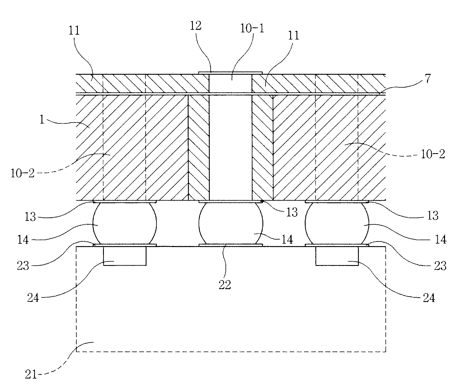
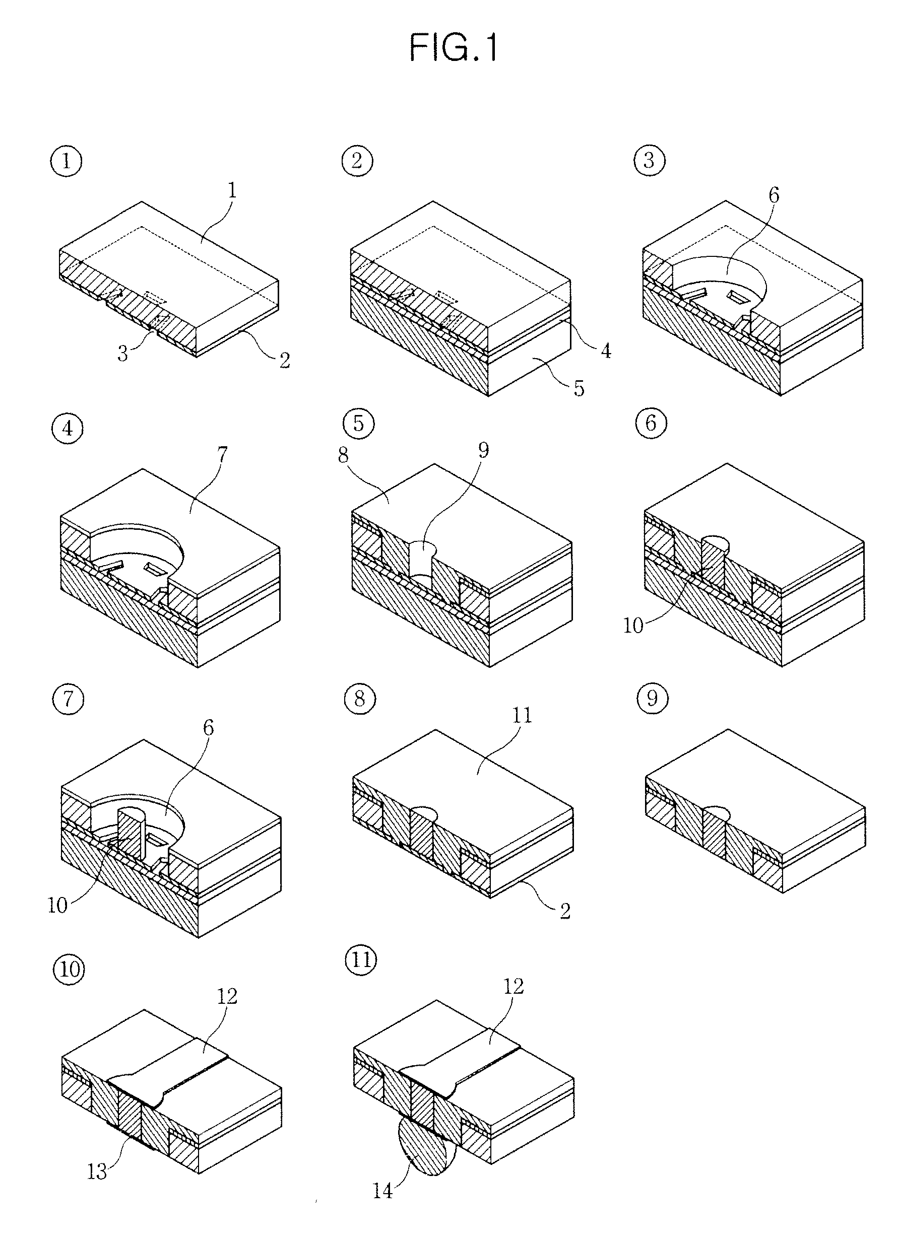
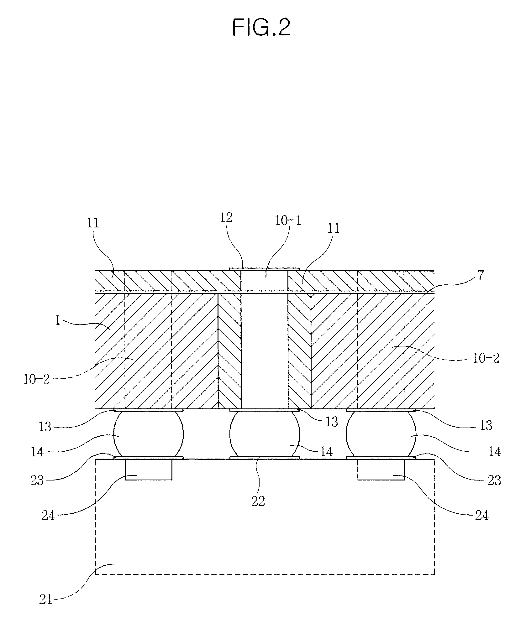
[0030]FIG. 1 shows a process of forming a through via having a thick insulating structure according to an exemplary embodiment of the present invention.

[0031]To begin with, a wafer 1 may be formed to a predetermined thickness. In the present specification, wafer refers to a semiconductor wafer or an insulating substrate. In an exemplary embodiment, the wafer 1 may be formed usi...


PUM


Abstract

A method of manufacturing a stacked semiconductor package using an improved technique of forming a through via in order to enable 3-dimensional vertical interconnection of stacked packages is provided. The method includes forming a seed layer required for forming a via core on a bottom surface of a wafer, forming at least one via hole vertically through the wafer, forming a via core in the via hole, insulating the via hole from the via core, and removing the seed layer from the bottom surface of the wafer. The stacked semiconductor package is suitable for high-speed signal transmission.

Description

CROSS REFERENCE TO RELATED APPLICATIONS[0001]This application claims priority from Korean Patent Application No. 10-2008-0081330, filed on Aug. 20, 2008, the disclosure of which is incorporated herein in its entirety by reference.BACKGROUND OF THE INVENTION[0002]1. Background of the Invention[0003]The present invention relates to a semiconductor packaging technique, and more particularly, to a 3-dimensional semiconductor packaging technique of connecting a plurality of chips by forming a hole vertically through a wafer without using a wire-bonding technique.[0004]2. Description of the Related Art[0005]Recent trends in micro-packaging technology reveal demand for inexpensive yet highly efficient, versatile yet smaller packaging. In order to meet such demand, a considerable amount of research has been conducted on new packaging techniques such as SoC (System-on-Chip), SiP (System-in-Package), MCM (Multi-Chip-Module), and SOP (System-on-Package) techniques. In particular, SOP technolog...

Claims


Application Information

Patent Timeline
Patent Type & Authority Applications(United States)
IPC IPC(8): H01L21/98H01L21/768
CPCH01L21/76898H01L23/481H01L25/50H01L2223/6616H01L2224/16H01L2225/06541H01L2924/09701H01L2924/3011H01L2225/06513H01L24/03H01L24/05H01L2224/0401H01L2224/05001H01L2224/05009H01L2224/05568H01L2224/0557H01L2224/056H01L2224/13025H01L2924/00014H01L2224/05099H01L23/12
Inventor LIM, KWON-SEOBSEO KANG, HYUN
Owner ELECTRONICS & TELECOMM RES INST
Why Eureka
Try Eureka