Semiconductor device

a technology of semiconductors and devices, applied in the direction of semiconductor/solid-state device details, instruments, fixed capacitors, etc., can solve the problems of increasing distance, affecting signal transmission speed, so as to reduce the impedance of wiring, reduce switching noise, and improve signal transmission speed

Inactive Publication Date: 2010-08-19
PS4 LUXCO SARL
View PDF37 Cites 6 Cited by
  • Summary
  • Abstract
  • Description
  • Claims
  • Application Information

AI Technical Summary

Benefits of technology

[0021]According to the present invention, the circuit excluding the data output circuit is supplied with the first power source potential or the first ground potential over the first path that passes through a prescribed conductive area on the semiconductor chip without routing the path around the semiconductor chip. Thus, the power source potential or the ground potential can be conducted through a wiring of a size that is close to that of a solid pattern and can be selected for the circuit excluding the data output circuit instead of a wiring routed around the semiconductor chip, and supplied over the linear path, thereby allowing the impedance of the wiring to be reduced. The data output circuit is supplied with the second power source potential or the second ground potential from the circuit board over the second path forming that forms the feedback current path. This reduces switching noise owing to switching of the output circuit, thereby enabling data signal transmission to be performed at higher speed.

Problems solved by technology

However, if the means disclosed in Japanese Patent Laid-Open No. 2004-327757 or 2003-332515 is used for a semiconductor device mounted with a semiconductor chip such as a DRAM, a problem arises in which speedup of the signal transmission is prevented even though impedances of the power source wiring and the ground wiring on the circuit board are reduced.
For example, when first power source wiring 240C1d is routed as shown in FIG. 5, a problem occurs in which the wire routing involves a long distance.
In addition, a problem unavoidable occurs in an area in which the width of the wire decreases, and further, there is an increase in the distance of the wire routing in order to keep the wire separate from each other.
As a result, the feedback current path of the output data signal by the second power source and ground system is distorted, and the effect of reducing switching noise decreases.

Method used


Image

  • Semiconductor device
  • Semiconductor device
  • Semiconductor device

Examples


first exemplary embodiment

[0051]Next, an exemplary embodiment will be described with reference to the drawings.

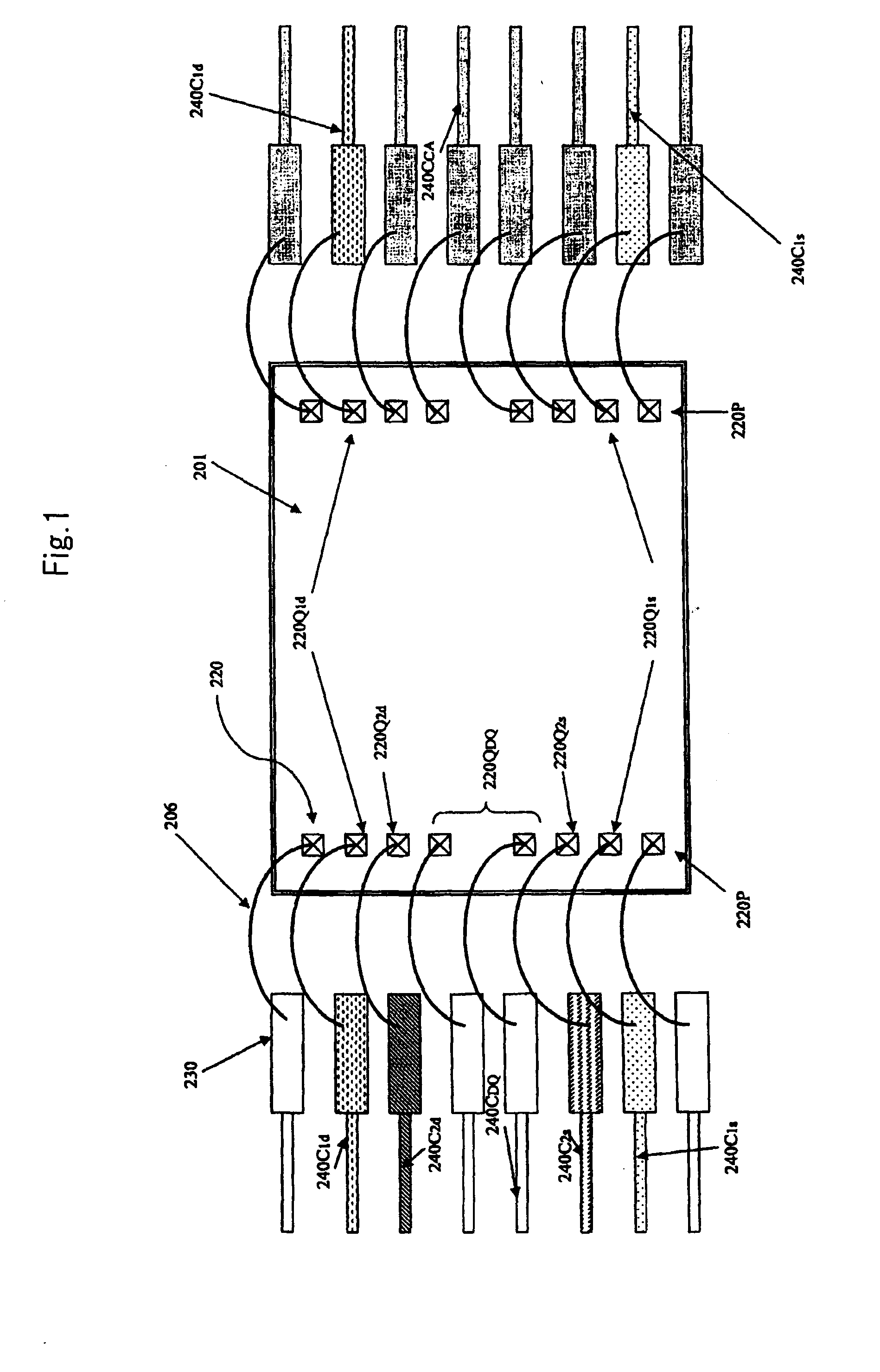
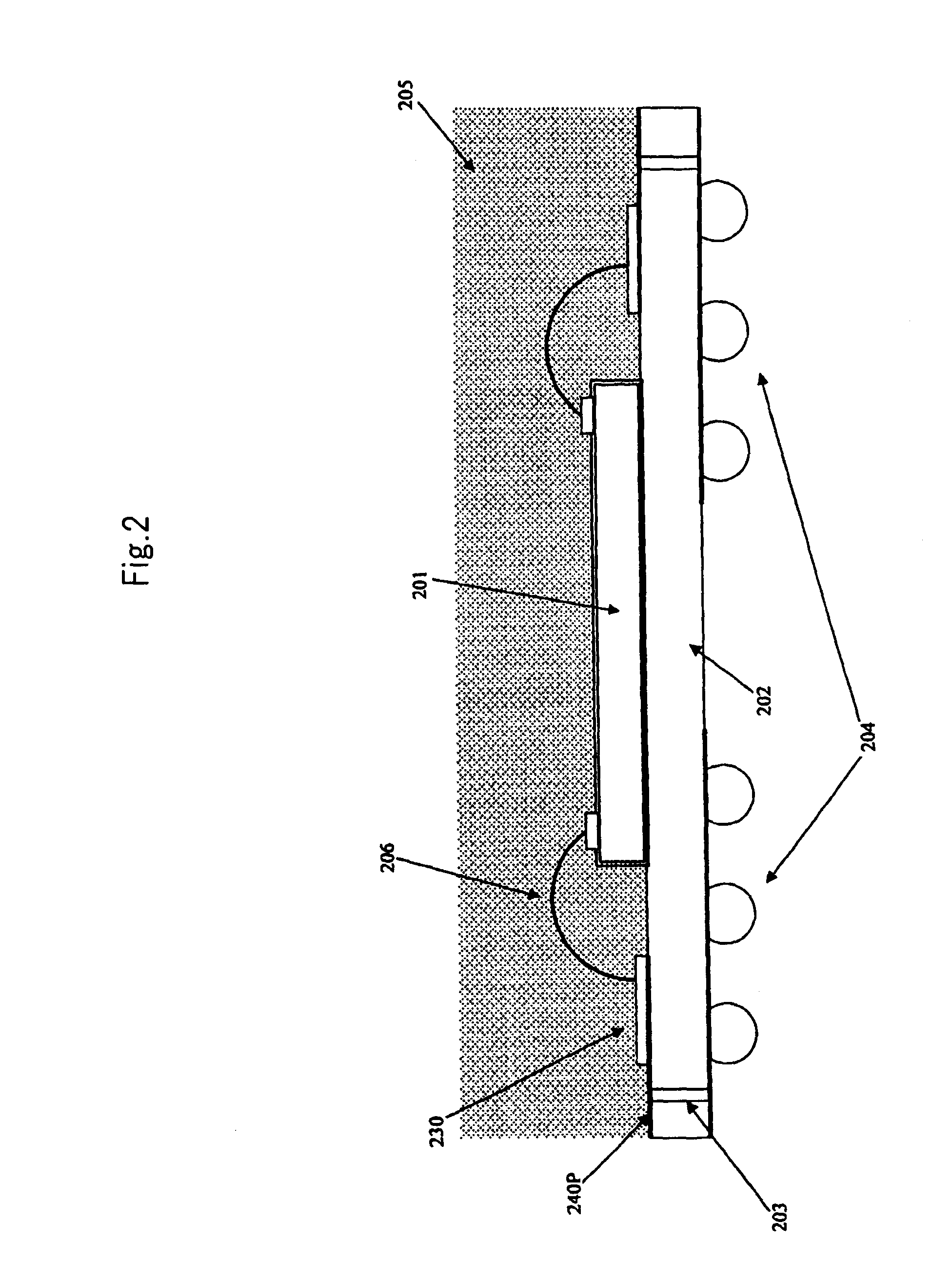
[0052]FIG. 6 is a schematic diagram showing a semiconductor chip of a semiconductor device according to the exemplary embodiment. FIG. 7 is a longitudinal sectional view of the semiconductor device shown in FIG. 6. FIG. 8 is a substrate wiring diagram of the semiconductor device viewed from a side of the semiconductor chip. FIG. 9 is a substrate wiring diagram of the semiconductor device viewed from a side of external terminals. FIG. 10 shows a block diagram of a data output circuit and the circuit excluding the data output circuit of the semiconductor chip according to the exemplary embodiment.

[0053]Note that “DQ system,” a term to be used in the following description, means a system used for data input and output, and “CA system” means a command / address system.

[0054]“First power source” and “VDD” indicate a power source (a first power supply potential) of the circuit excluding the data output circ...

second exemplary embodiment

[0125]Next, FIG. 22 shows a schematic view of semiconductor chip of a semiconductor device according to another exemplary embodiment. FIG. 23 shows a longitudinal sectional view of the semiconductor device shown in FIG. 22.

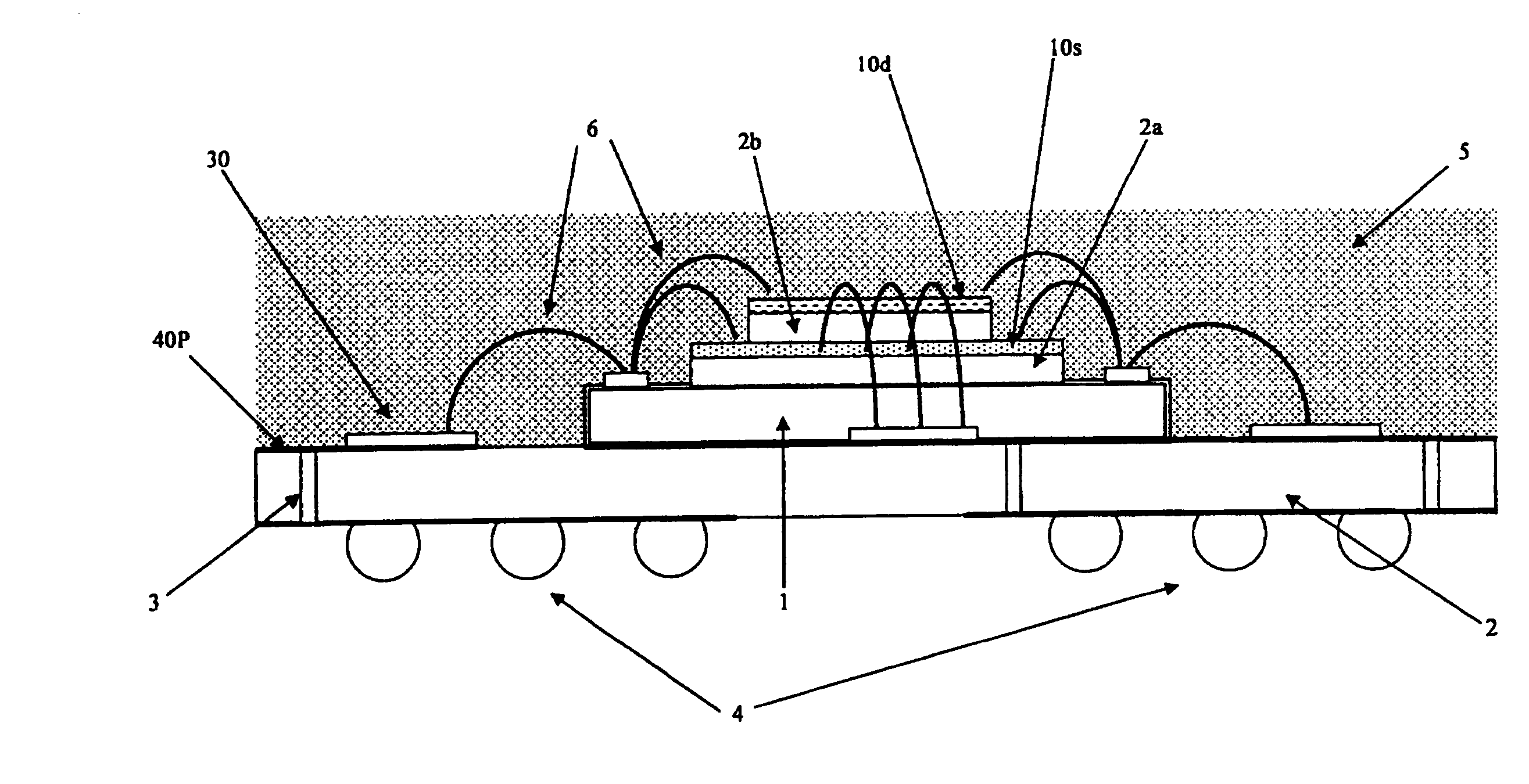
[0126]The semiconductor device according to the first embodiment shown in FIGS. 6 and 7 adopts the configuration where additional substrate 2a is provided on semiconductor chip 1 and additional substrate 2b is provided in a stacked manner on additional substrate 2a. In this configuration, first additional wiring layer for ground 10s is formed on the upper surface of additional substrate 2a, and first additional wiring layer for power source 10d is formed on additional substrate 2b. The semiconductor device according to the first exemplary embodiment thus adopts the configuration where the additional wiring layers are formed on the two stacked additional substrates, respectively.

[0127]On the other hand, in a configuration shown in FIGS. 22 and 23, first additional ...

third exemplary embodiment

[0128]A configuration shown in FIGS. 24 to 26 is different in that second semiconductor chip 1b is provided between semiconductor chip 1 (first semiconductor chip 1a) and additional wiring substrate 2a compared to the semiconductor device of the first exemplary embodiment shown in FIGS. 6, 7 and 10. More specifically, in a semiconductor device of this exemplary embodiment, second semiconductor chip 1b is provided on first semiconductor chip 1a disposed on wiring substrate 2. Additional substrate 2a is provided on second semiconductor chip 1b. Additional substrate 2b is further provided stacked on this additional substrate 2a. First semiconductor chip 1a includes electrode pads 20a, as with the first exemplary embodiment. These electrode pads 20a include CA system signal pads 20ACAa connected to other circuit 7ba excluding data output circuits 7aa provided on semiconductor chip 1a, first power source pads 20Q1da supplying other circuit 7ba with a potential of one side of a first powe...


PUM


Abstract

A semiconductor device reduces the impedance of a wiring for supplying the circuit excluding a data output circuit with a power source voltage or a ground voltage and of speedup of data signal transmission in the data output circuit. Additional substrates 2a, 2b are on the upper surface of semiconductor chip 1. First additional wiring layer for power source 10d and first additional wiring layer for ground 10s formed on respective additional substrates 2a, 2b form prescribed conductive areas on semiconductor chip 1. First power source wiring 40C1d or first ground wiring 40C1s are interconnected through additional wiring layers 10d and 10s. Second power source wiring 40C2d and second ground wiring 40C2s, which is extended in the same direction as with DQ system signal wiring 40CDQ, forms a feedback current path. Second power source wiring 40C2d and second ground wiring 40C2s are disposed adjacent to DQ system signal wiring 40CDQ.

Description

[0001]This application is based upon and claims the benefit of priority from Japanese patent application No. 2009-35546, filed on Feb. 18, 2009, the disclosure of which is incorporated herein in its entirety by reference.BACKGROUND OF THE INVENTION[0002]1. Field of the Invention[0003]The present invention relates to a semiconductor device including a power source wiring and a ground wiring.[0004]2. Description of the Related Art[0005]In recent years, a technique that reduces unevenness in the potential of electrode pads for a power source or in the potential of electrodes pads for a ground of the semiconductor chip has been utilized. This realizes a semiconductor device with increased electric properties. In such semiconductor device, for example, a power source voltage for the electrode pads for the power source is supplied from a common power source wiring in a package substrate, and a ground voltage for the electrode pads for the ground is supplied from a common ground wiring in ...

Claims


Application Information

Patent Timeline
Patent Type & Authority Applications(United States)
IPC IPC(8): H05K7/00
CPCH01L23/49816H01L23/49827H01L23/50H01L25/0657H01L25/18H01L2224/32145H01L2224/48091H01L2224/48227H01L2224/48247H01L2224/49175H01L2225/0651H01L2225/06517H01L2924/0102H01L2924/15311H01L2924/3011H01L24/48H01L24/49H01L2224/48145H01L2224/73265H05K1/181H01L2224/32225H01L2924/30107G11C5/063H01L2924/00014H01L2924/00H01L2924/00012H01L24/73H01L2924/181H01L2224/05554H01L2224/45099H01L2224/45015H01L2924/207
Inventor ITAYA, SATOSHIISA, SATOSHIKATAGIRI, MITSUAKISASAKI, DAI
Owner PS4 LUXCO SARL
Why Eureka
Try Eureka