
Power MOSFET device structure for high frequency applications

a power mosfet and high frequency technology, applied in the field of device configuration and fabrication process of power mosfet device structure, can solve the problems of difficult to reduce the cell size, and limited conventional device configuration and manufacturing process of power switching device, so as to reduce the gate-drain overlapping area, reduce the input and feedback capacitance, and reduce the overlapping area

Active Publication Date: 2006-11-09
ALPHA & OMEGA SEMICON LTD
View PDF13 Cites 54 Cited by
  • Summary
  • Abstract
  • Description
  • Claims
  • Application Information

AI Technical Summary

Benefits of technology

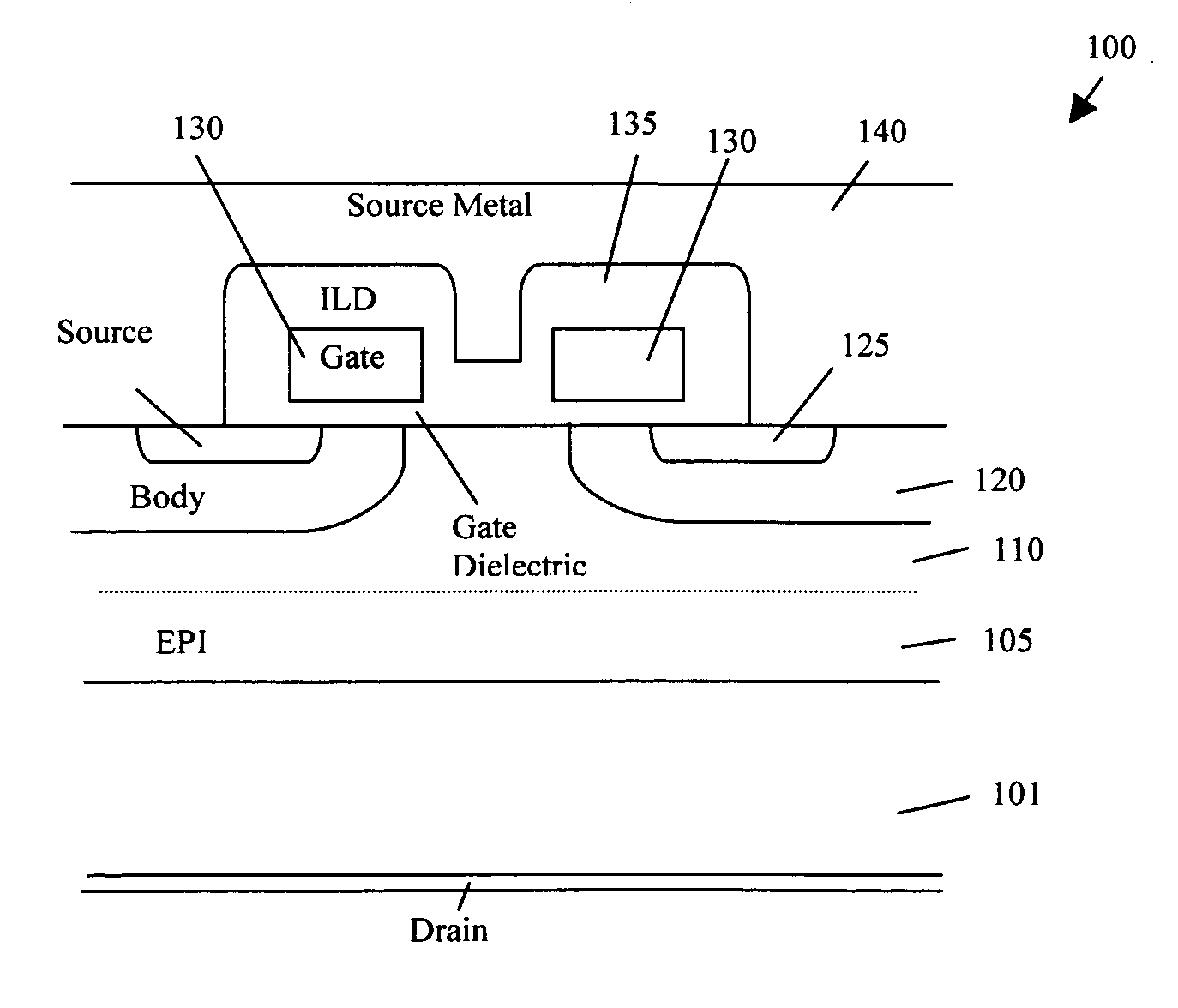
[0009] It is therefore an object of the present invention to provide an improved MOSFET device with a reduced gate-drain capacitance by first reducing the gate-drain overlapping area with a specially configured gate. The gate is patterned as splitted gate with interposing bore for depositing a source metal into the interposing cavity. The gate is further insulated with dielectric layer having a predefined thickness to reduce the input and feedback capacitance to improve the transient efficiency for better switching performance.
[0010] Specifically, it is an object of the present invention to provide an improved MOSFET device with a novel configuration by interposing a source metal into a gate electrode for achieving dual purposes of reducing the overlapping area between the gate and drain and to preventing electric field coupling between the gate and the epitaxial layer underneath the gate thus significant reduce the gate to drain capacitance. Higher switching speed and reduced transient losses are achieved with the improved switching device disclosed in this invention.
[0011] Briefly in a preferred embodiment this invention discloses a vertical power device supported on a semiconductor that includes a drain disposed on a first surface and a source region disposed near a second surface of the semiconductor opposite said first surface. The vertical power device further includes an insulated gate electrode disposed on top of the second surface for controlling a source to drain current. A source electrode is interposed into the insulated gate electrode for substantially preventing a coupling of an electrical field between the gate electrode and an epitaxial region underneath the insulated gate electrode. The source electrode further covers and extends over the insulated gate for covering an area on the second surface of the semiconductor to contact the source region. The semiconductor substrate further includes an epitaxial layer disposed above and having a different dopant concentration than the drain region. The insulated gate electrode further includes an insulation layer for insulating the gate electrode from the source electrode wherein the insulation layer has a thickness that is depending on a Vgsmax rating of the vertical power device. In another preferred embodiment, the insulated gate electrode further includes an insulation layer for insulating the gate electrode from the source electrode and the insulation layer has a greater thickness surrounding an outer edge of the gate electrode for allowing an alignment tolerance for etching a contact opening. In a preferred embodiment, a vertical power device further includes an N-channel MOSFET cell. In another preferred embodiment, a vertical power device further includes a P-channel MOSFET cell.

Problems solved by technology

As there is an ever growing demand for high frequency switch power devices, conventional device configurations and manufacturing processes of power switching devices are still limited by speed-limiting capacitance between the gate and drain of the power transistors, e.g., MOSFET and IGBT.
However, such device configurations still have problems and limitations.
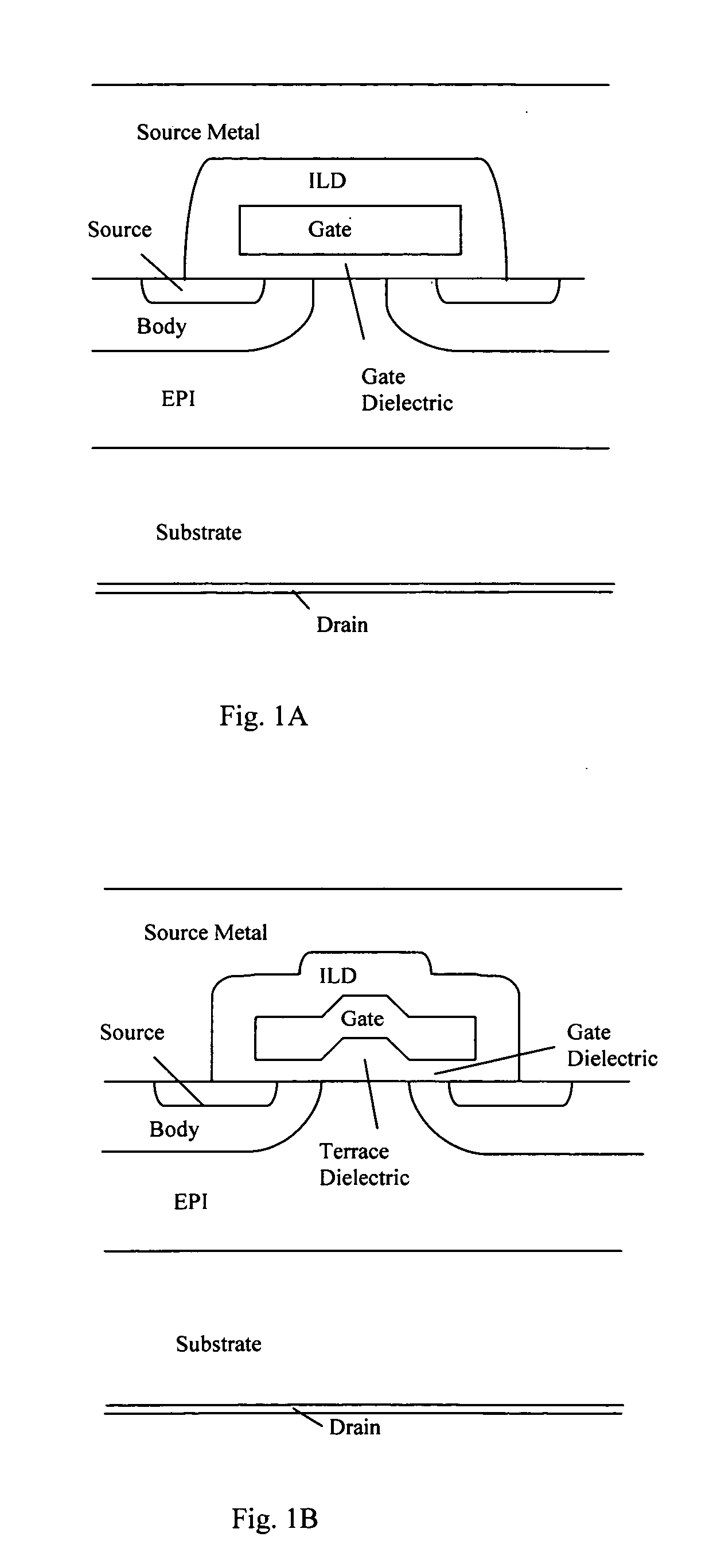
One problem with the terrace gate-oxide design is that the process is not self-aligned; therefore it is hard to reduce the cell size.
A second problem for this design is that the thick terrace dielectric layer reduces the accumulation of carrier in the drain area under the dielectric terrace and this increases the Rdson of the device.
Furthermore, the reduction of Crss is limited by the thickness of the terrace dielectric.
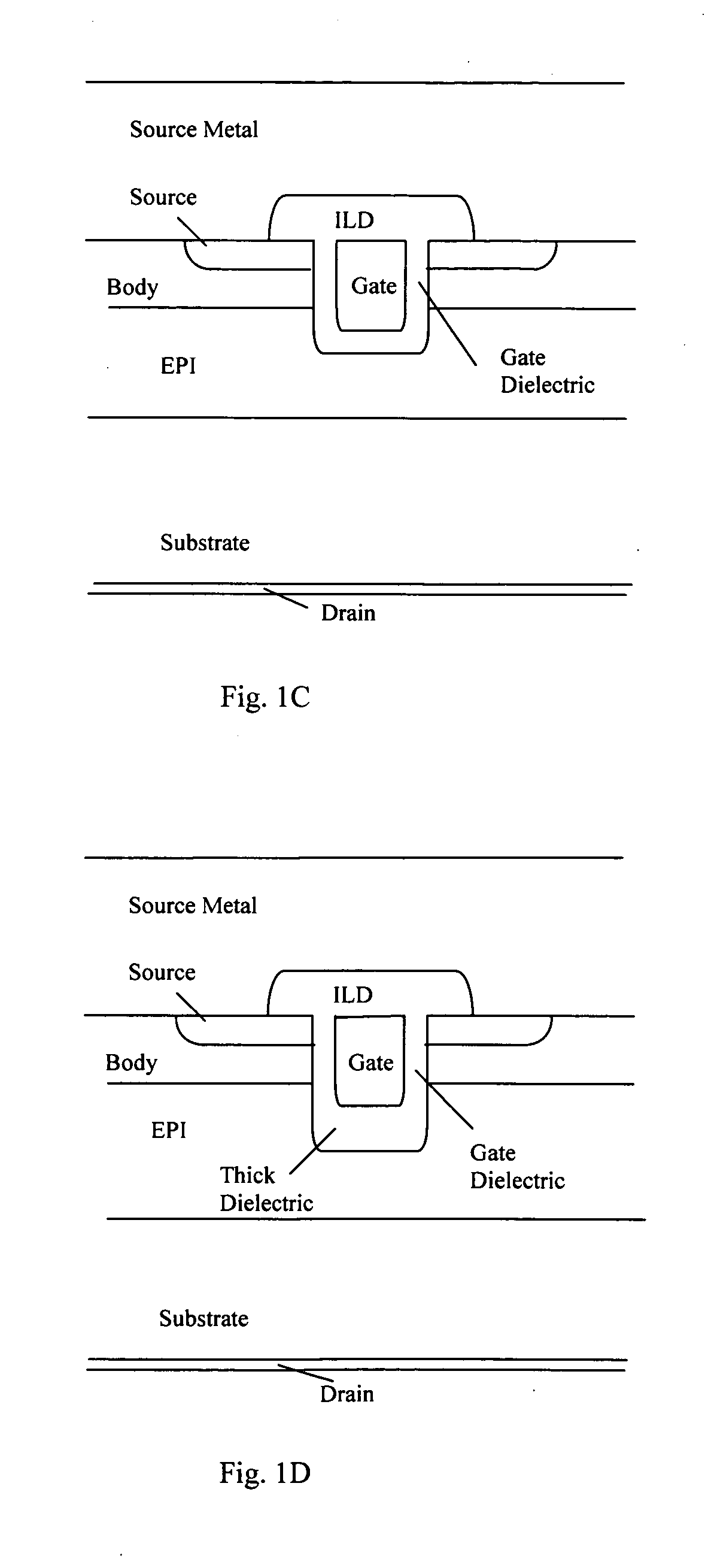
This is especially true for the thick trench bottom oxide approach in trench device where the thick bottom oxide is hard to make.
However, with the split gate configuration, there are still some fringing electric field couplings between the gate electrodes to the epitaxial layer connecting to the drain electrode.

Method used


Image

  • Power MOSFET device structure for high frequency applications
  • Power MOSFET device structure for high frequency applications
  • Power MOSFET device structure for high frequency applications

Examples


Embodiment Construction

[0029] Referring to FIG. 2 for an equivalent circuit of a MOSFET device M includes a gate, drain and source electrodes wherein the gate has a gate resistance Rg and there is an adjustable resistance over the epitaxial layer and the substrate connected to the drain electrode. A PN diode, e.g., Dbody, is formed across the body layer. There are capacitors between three electrodes, i.e., Cgs between the gate and the source, Cgd between the gate and the drain and Cds between the drain and the source. In the power MOSFET parlance, the input capacitance Ciss, feedback capacitance Crss and output capacitance Coss are determinate by the follows:

Ciss=Cgd+Cgs

Crss=Cgd

Coss=Cds+Crss

[0030] The input capacitance Ciss is inversely proportional to the achievable maximum frequency the MOSFET device can operate. Therefore, in order to increase the operation frequency, a design approach is to reduce the input capacitance Ciss.

[0031] Furthermore, the input capacitance Ciss and the feedback capacitan...


PUM


Abstract

This invention discloses a new switching device supported on a semiconductor that includes a drain disposed on a first surface and a source region disposed near a second surface of said semiconductor opposite the first surface. The switching device further includes an insulated gate electrode disposed on top of the second surface for controlling a source to drain current. The switching device further includes a source electrode interposed into the insulated gate electrode for substantially preventing a coupling of an electrical field between the gate electrode and an epitaxial region underneath the insulated gate electrode. The source electrode further covers and extends over the insulated gate for covering an area on the second surface of the semiconductor to contact the source region. The semiconductor substrate further includes an epitaxial layer disposed above and having a different dopant concentration than the drain region. The insulated gate electrode further includes an insulation layer for insulating the gate electrode from the source electrode wherein the insulation layer having a thickness depending on a Vgsmax rating of the vertical power device.

Description

BACKGROUND OF THE INVENTION [0001] 1. Field of the Invention [0002] The invention disclosed herein relates generally to the device configuration and fabrication process of semiconductor switching devices. More particularly, this invention relates to a novel and improved device configuration and fabrication process for providing high frequency power switching devices. [0003] 2. Description of the Prior Art [0004] As there is an ever growing demand for high frequency switch power devices, conventional device configurations and manufacturing processes of power switching devices are still limited by speed-limiting capacitance between the gate and drain of the power transistors, e.g., MOSFET and IGBT. There is an urgent need to overcome such limitations especially when high frequency switching power supplies are providing power to wide range of electronic devices. [0005] Referring to FIGS. 1A to 1D for conventional techniques as that shown in FIGS. 1B and 1D for reducing the gate-drain c...

Claims


Application Information

Patent Timeline
IPC IPC(8): H01L29/78H01L21/336
CPCH01L29/0878H01L29/402H01L29/41741H01L29/41775H01L29/42372H01L29/7827H01L29/66719H01L29/66727H01L29/7802H01L29/7811H01L29/42376
Inventor BHALLA, ANUPNG, DANIELLI, TIESHENGLUI, SIK K.
Owner ALPHA & OMEGA SEMICON LTD
Learn More