Pixel array, active device array substrate and flat display panel

a technology of active devices and substrates, which is applied in the direction of discharge tubes luminescnet screens, instruments, printed circuit non-printed electric components association, etc., can solve the problems of reducing the usable area of storage capacitors, affecting the affecting etc., to achieve satisfactory performance of storage capacitors cst and other devices, the effect of improving the quality of display images

Active Publication Date: 2013-01-10
AU OPTRONICS CORP
View PDF1 Cites 10 Cited by
  • Summary
  • Abstract
  • Description
  • Claims
  • Application Information

AI Technical Summary

Benefits of technology

[0009]The invention is directed to a pixel structure, an active device array substrate having the pixel structure, and a flat display panel. In th...

Problems solved by technology

As mentioned above, the devices in the FPD operated under a high voltage may have increasing current leakage.
However, to ensure satisfactory electrical performance of the pixel structure P (e.g., to reduce the current leakage and increase the conductive current), the layout design of two serially-connected TFTs needs to be applied in the pixel structure P. The increasing number of TFTs leads to reduction of the usable area of the storage capacitor Cst, and thus the storage capacitance of the storage capacitor Cst ca...

Method used


Image

  • Pixel array, active device array substrate and flat display panel
  • Pixel array, active device array substrate and flat display panel
  • Pixel array, active device array substrate and flat display panel

Examples


Embodiment Construction

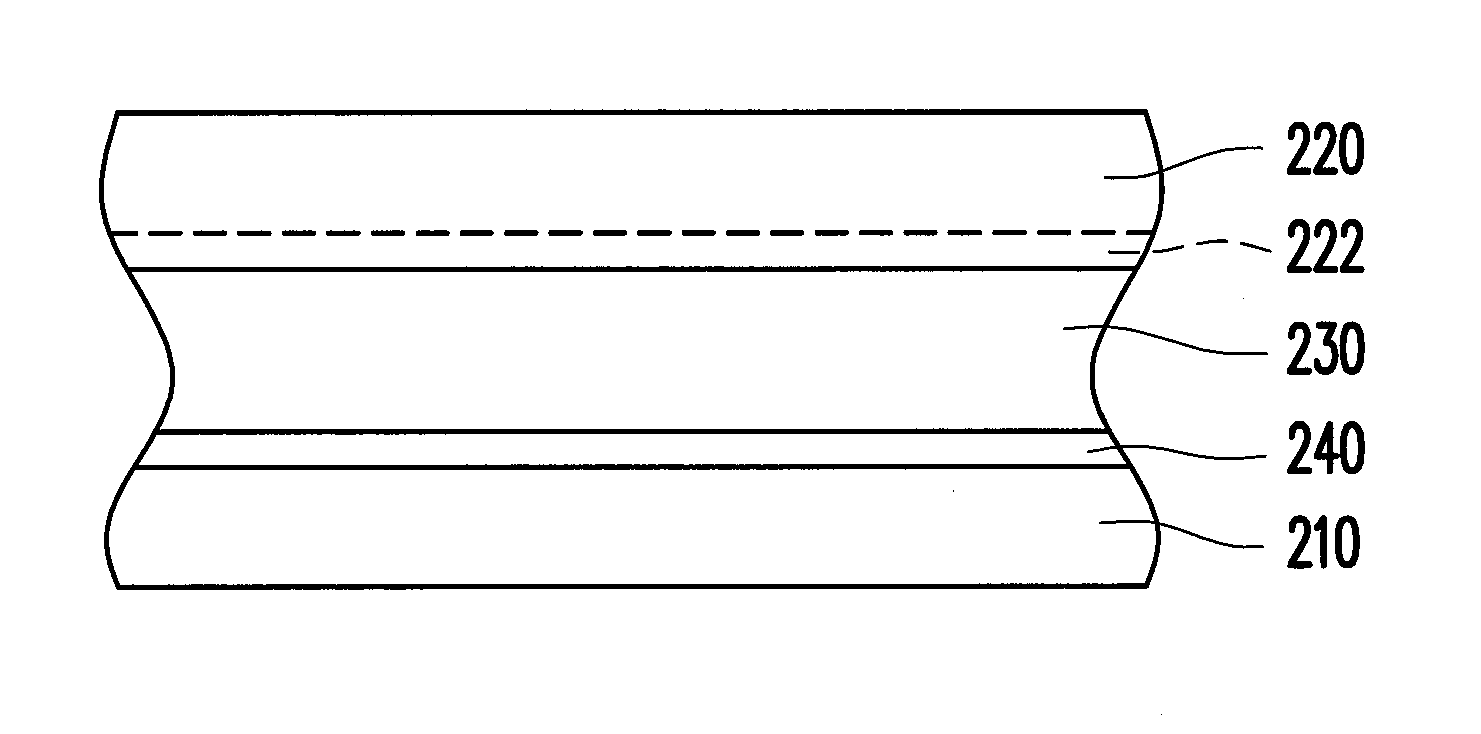
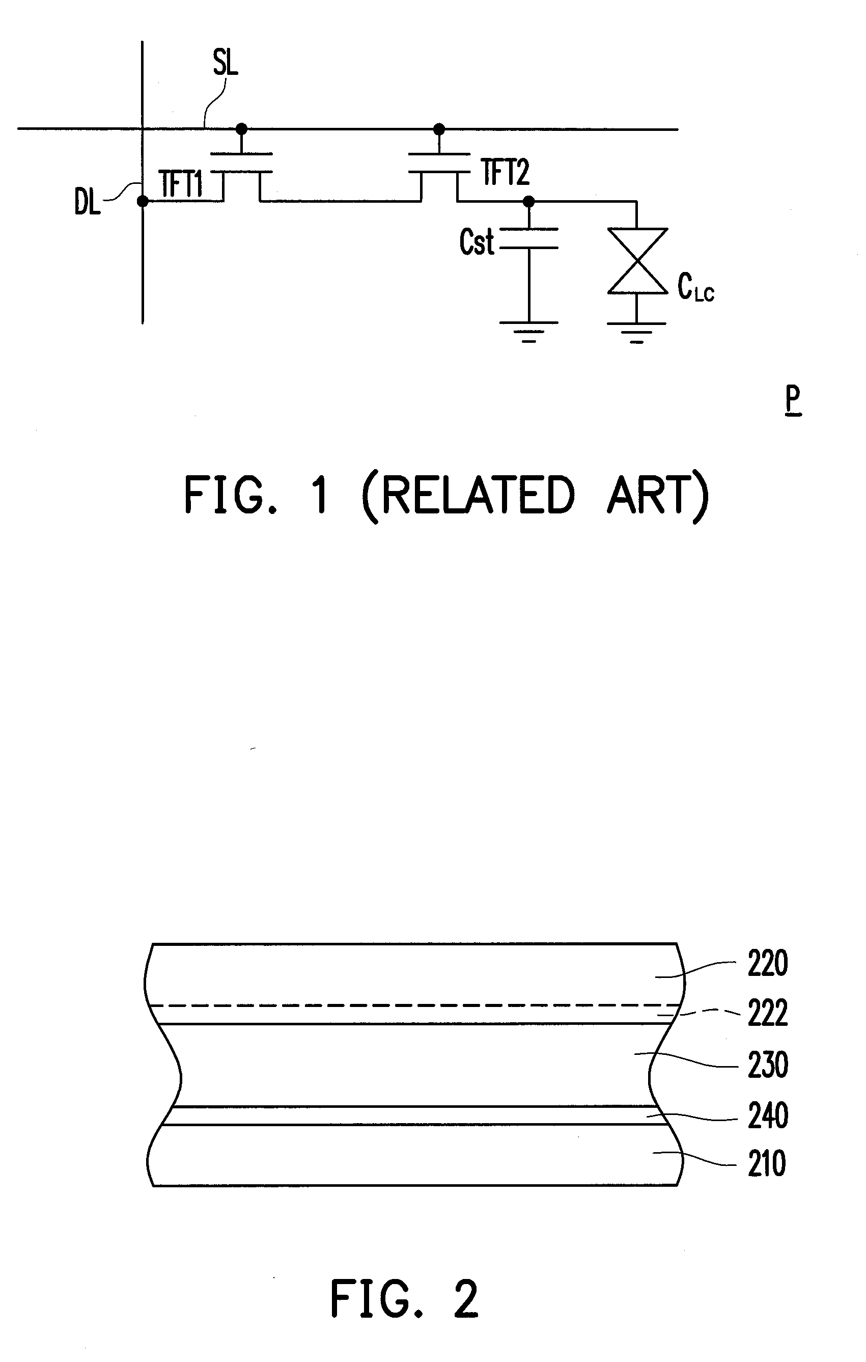
[0045]FIG. 2 is a schematic cross-sectional view illustrating a flat display panel according to an embodiment of the invention. With reference to FIG. 2, the flat display panel includes a first substrate 210, a second substrate 220, a display medium 230, and an active device array 240. The second substrate 220 is located above the first substrate 210. Here, the second substrate 220 can be a simple blank substrate or a substrate that includes an opposite electrode 222. The display medium 230 is located between the first substrate 210 and the second substrate 220. The display medium 230 is an electro-phoretic display film, an organic electroluminescent layer, or a liquid crystal layer, for instance, and the electro-phoretic display film can be a microcup electro-phoretic display film or a microcapsule electro-phoretic display film. This is well known to people having ordinary skill in the art, and thus no further description is given below. The active device array 240 is configured on...


PUM


Abstract

A pixel array including a pixel electrode and an active device is provided. The active device includes a gate, a channel layer, a source, a drain, a connection electrode, a first branch portion and a second branch portion. The gate is electrically connected with a scan line. The channel layer located at a side of the gate is electrically isolated from the gate. The source, the drain and the connection electrode are disposed on a part region of the channel layer. The first branch portion disposed on a part region of the channel layer is connected with an end of the connection electrode. The first branch portion surrounds the source located on the channel layer. The second branch portion disposed on a part region of the channel layer is connected with the other end of the connection electrode. The second branch portion surrounds the drain located on the channel layer.

Description

CROSS-REFERENCE TO RELATED APPLICATION[0001]This application claims the priority benefit of Taiwan application serial no. 100123889, filed on Jul. 6, 2011. The entirety of the above-mentioned patent application is hereby incorporated by reference herein and made a part of this specification.BACKGROUND OF THE INVENTION[0002]1. Field of the Invention[0003]The invention relates to a pixel structure, an active device array substrate having the pixel structure, and a flat display panel.[0004]2. Description of Related Art[0005]With increasing progress towards display technologies, displays facilitate our daily lives, and the requirements for light and compact displays contribute to development of flat panel displays (FPDs) as the mainstream displays at this current stage. In general, each pixel structure in an FPD includes an active device and a pixel electrode, and the active device serves as a switch element of a display unit. To control each individual pixel structure, a certain pixel ...

Claims


Application Information

Patent Timeline
IPC IPC(8): G02F1/1343H05B33/14G02B26/00H05K1/18
CPCG02F1/13624H01L27/124H01L29/41733
Inventor WEI, CHUAN-SHENGCHIANG, MING-TAOLIN, YU-TINGCHEN, MAW-SONGHUANG, WEI-MING
Owner AU OPTRONICS CORP
Why Eureka
Try Eureka