Level converter circuit and a liquid crystal display device employing the same

a level converter and liquid crystal display technology, applied in logic circuit coupling/interface arrangement, pulse technique, instruments, etc., can solve the problems of many mos transistors, inability to obtain sufficient driving capability in a case, and level converter circuits that had many mos transistors, etc., to achieve high speed and stably irrespective

Inactive Publication Date: 2006-04-13
PANASONIC LIQUID CRYSTAL DISPLAY CO LTD +1
View PDF4 Cites 31 Cited by
  • Summary
  • Abstract
  • Description
  • Claims
  • Application Information

AI Technical Summary

Benefits of technology

[0046] The present invention is made so as to solve the above problems with the prior art, it is an object of the present invention to provide a technique capable of operating a level converter circuit at a high speed and stably irrespective of variations of threshold voltages of transistors.
[0047] It is another object of the present invention to provide a technique capable of improving the quality of displayed images by a liquid crystal display device by using the above level converter circuit.

Problems solved by technology

The level converter circuit shown in FIG. 13 needs a total of eight MOS transistors comprising four MOS transistors M5 to M8 in the low-voltage circuit and four MOS transistors M9 to M12 in the high-voltage circuit, the level converter circuit shown in FIG. 14 needs six MOS transistors, and therefore the prior art level converter circuits had the problem in that many MOS transistors are needed.
As a result, when the level converter circuits shown in FIGS. 13 and 14 are formed by MOS transistors having semiconductor layers made of single crystal silicon, satisfactory operation can be guaranteed, but when the level converter circuits shown in FIGS. 13 and 14 are formed by polysilicon MOS transistors having semiconductor layers made of polysilicon, there was a disadvantage that sufficient driving capability could not be obtained in a case where the supply voltage is the low voltage VCC.
As a result, if the prior art level converter circuit is formed by polysilicon MOS transistors, the DC transfer characteristics of the CMOS inverters INV1, INV2 (see FIG. 13) vary greatly mainly due to the variations of the threshold voltages VTH of the polysilicon MOS transistors of the CMOS inverters INV1, INV2, and consequently, there was a problem in that a delay time (or a phase difference) of the output signal with respect to the input signal and a variation of a duration of the H or L level of the output signal increase.
In a liquid crystal display module of the analog-sampling active-matrix type using polysilicon MOS transistors, such variations of the delay time of the output signal from the level converter circuit and the duration of the H level of the output signal cause a degradation in picture quality such as a picture defect in the form of a vertical line, when a half tone picture is displayed.
These produce a ghost in an image displayed on a liquid crystal display panel, and therefore deteriorate display quality of the displayed image extremely.

Method used


Image

  • Level converter circuit and a liquid crystal display device employing the same
  • Level converter circuit and a liquid crystal display device employing the same
  • Level converter circuit and a liquid crystal display device employing the same

Examples


embodiment 1

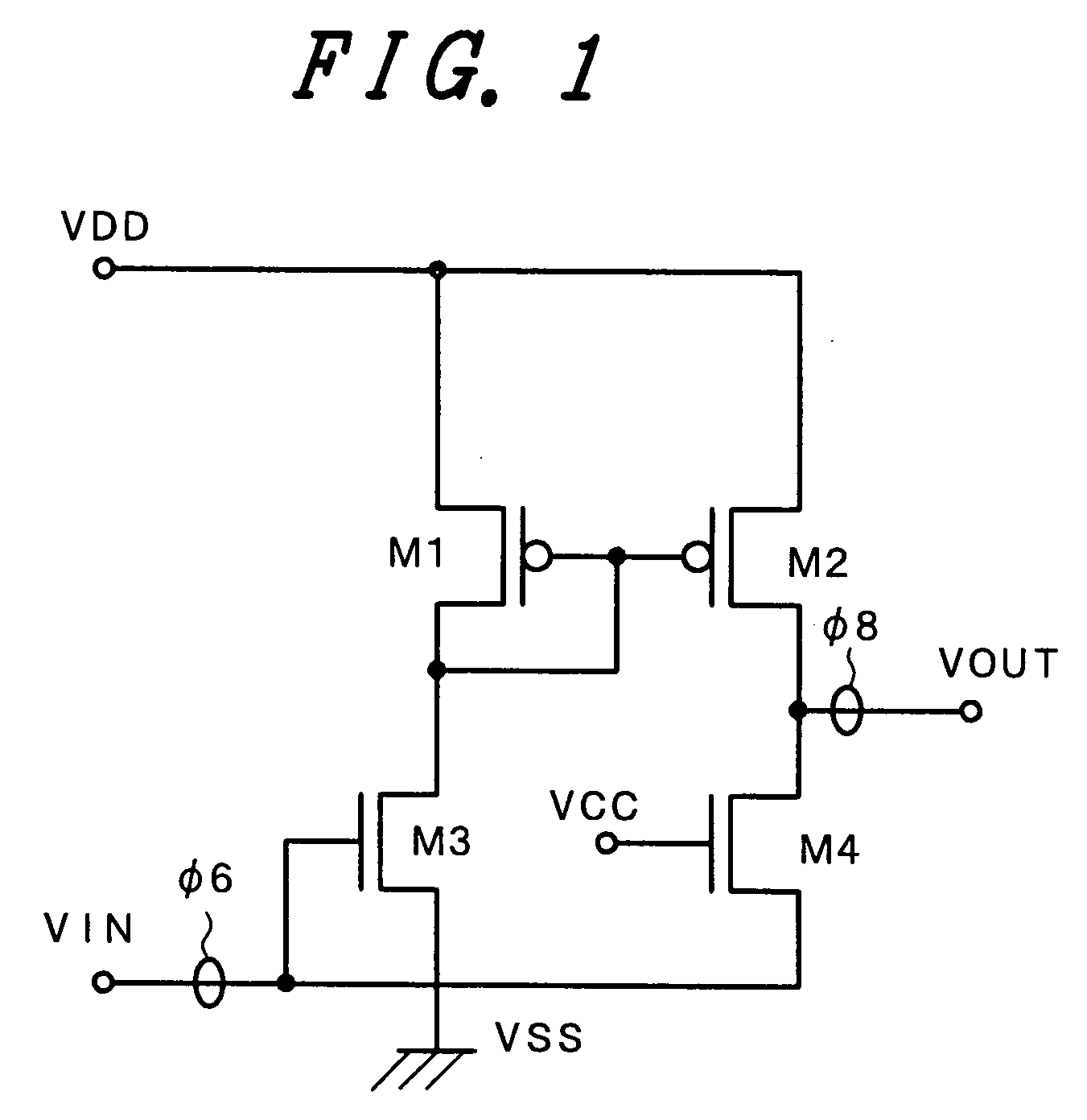
[0077]FIG. 1 is a circuit diagram representing a level converter circuit of Embodiment 1 of the present invention.

[0078] As shown in FIG. 1, the level converter circuit of this embodiment is formed by a total of transistors including two enhancement-mode p-channel polysilicon MOS transistors and two enhancement-mode n-channel polysilicon MOS transistors, and the level converter circuit has a first stage formed by PMOS M1 and NMOS M3 and a second stage formed by PMOS M2 and NMOS M4.

[0079] A source electrode of NMOS M3 of the first stage is connected to the reference voltage VSS (ground potential) and a gate electrode of NMOS M3 is supplied with an input signal φ6 from a input terminal VIN.

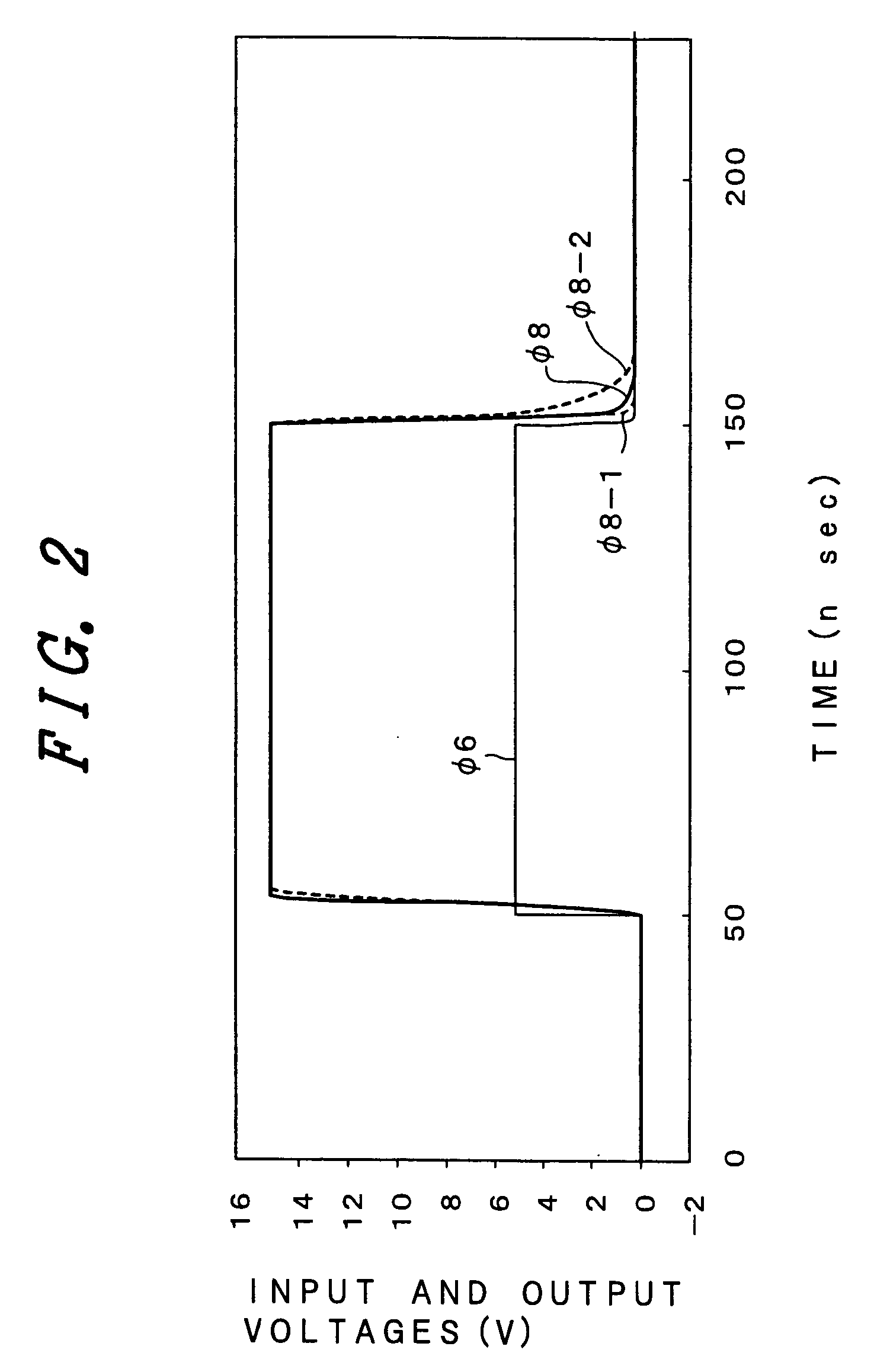
[0080] The input signal φ6 has an amplitude of VCC, or varies from a voltage higher than VCC to ground potential VSS.

[0081] A drain electrode of PMOS M1 is connected to a drain electrode of NMOS M3, and a source electrode and a gate electrode of PMOS M1 are connected to the high voltage VDD and ...

embodiment 2

[0103]FIG. 8 is a circuit diagram of a level converter circuit of Embodiment 2 of the present invention.

[0104] As shown in FIG. 8, the level converter circuit of this embodiment also uses a total of four enhancement-mode transistors including two p-channel polysilicon MOS transistors and two n-channel polysilicon MOS transistors, and has the first stage formed by PMOS M1 and NMOS M3 and the second stage formed by PMOS M2 and NMOS M4.

[0105] The level converter circuit of this embodiment differs from that of Embodiment 1, in that a source electrode of NMOS M3 of the first stage is supplied with the input signal φ6, a gate electrode of NMOS M3 is connected to the low voltage VCC, a source electrode of NMOS M4 of the second stage is connected to the reference voltage VSS and a gate electrode of NMOS M4 is supplied with the input signal φ6 from the input terminal VIN.

[0106] In the level converter circuit of this embodiment, when the input signal φ6 from the input terminal VIN is at th...

embodiment 3

[0114]FIG. 9 is a circuit diagram of a level converter circuit of Embodiment 3 of the present invention.

[0115] As shown in FIG. 9, the level converter circuit of this embodiment also uses a total of four enhancement-mode transistors including two p-channel polysilicon-MOS transistors and two n-channel polysilicon MOS transistors, and has the first stage formed by PMOS M1 and NMOS M3 and the second stage formed by PMOS M2 and NMOS M4.

[0116] The level converter circuit of this embodiment differs from that of Embodiment 1, in that a gate electrode of PMOS M1 of the first stage is connected to a drain electrode (i.e., the output terminal VOUT) of PMOS N2 of the second stage.

[0117] In the level converter circuit of this embodiment, when the input signal φ6 from the input terminal VIN is at the H level, NMOS M3 is ON, PMOS M1 is OFF, NMOS M4 is OFF, PMOS M2 is ON, and therefore the output terminal VOUT outputs the high voltage VDD.

[0118] Next, when the input signal oh 6 is at the L le...


PUM

PropertyMeasurementUnit
softening temperatureaaaaaaaaaa
threshold voltageaaaaaaaaaa

Abstract

A display device includes a pixel driver circuit. Each of level converter circuits in the pixel driver circuit has: an input terminal supplied with a signal swinging between a first voltage and a second voltage lower than the first voltage; a first first-conductivity-type transistor having a gate electrode coupled to the input terminal, and a source region coupled to ground; a second second-conductivity-type transistor having a gate electrode coupled to a drain region of the first transistor, a source region coupled to a power supply, and a drain region coupled to an output terminal; one circuit element among a diode, a resistor and a fourth second-conductivity-type transistor, coupled between the gate electrode of the second transistor and the power supply; a third first-conductivity-type transistor having a source region coupled to the input terminal, a drain region coupled to the output terminal, and a gate electrode supplied with a dc voltage.

Description

CROSS-REFERENCE TO RELATED APPLICATIONS [0001] This application is a Continuation application of U.S. application Ser. No. 10 / 460,154 filed Jun. 13, 2003, which is a Continuation application of U.S. application Ser. No. 09 / 780,492 filed Feb. 12, 2001. Priority is claimed based on U.S. application Ser. No. 10 / 460,154 filed Jun. 13, 2003, which claims priority to U.S. application Ser. No. 09 / 780,492 filed Feb. 12, 2001, which claims priority to Japanese Patent Application No. 2000-047164 filed on Feb. 24, 2000, all of which is incorporated by reference.BACKGROUND OF THE INVENTION [0002] The present invention relates to a level converter circuit and a liquid crystal display device employing the level converter circuit, and in particular to a level converter circuit formed by polysilicon transistors. [0003] Liquid crystal display modules of the STN (Super Twisted Nematic) type or the TFT (Thin Film Transistor) type are widely used as a display device for a notebook personal computer and...

Claims


Application Information

Patent Timeline
Patent Type & Authority Applications(United States)
IPC IPC(8): G09G5/00G02F1/136G02F1/133G02F1/1368G09G3/36H03K19/003H03K19/0185
CPCG09G3/3648G09G3/3677G09G2300/0408G09G2310/0289H03K19/00384H03K19/018571G09G3/36
Inventor OKUMURA, HARUHISAODE, YUKIHIDE
Owner PANASONIC LIQUID CRYSTAL DISPLAY CO LTD
Why Eureka
Try Eureka