Liquid crystal display device

a liquid crystal display and display device technology, applied in semiconductor devices, instruments, optics, etc., can solve the problems of reduced on-screen image viewability, inability to accept small-sized equipment, and electric power consumption, and achieve excellent on-screen display image quality, high production yield, and high aperture ratio

Inactive Publication Date: 2005-05-10
PANASONIC LIQUID CRYSTAL DISPLAY CO LTD +1
View PDF6 Cites 36 Cited by
  • Summary
  • Abstract
  • Description
  • Claims
  • Application Information

AI Technical Summary

Benefits of technology

[0011]It is therefore an object of the present invention to provide a new and improved structure of a partially transmissive and partially reflective liquid crystal display device c

Problems solved by technology

However, electrical power being consumed by the backlight is ordinarily more than 50% of total power consumed by the liquid crystal panel, and is impermissible for small size equipment such as portable telephones, mobile information terminals or the like.
These liquid crystal display device of the reflection type are faced with a problem as to a decrease in on-screen image viewability in cases where ambient light is dark.
The related art liquid crystal display devices of the partial transmission/reflection or “transflective” type are enc

Method used


Image

  • Liquid crystal display device
  • Liquid crystal display device
  • Liquid crystal display device

Examples


first embodiment

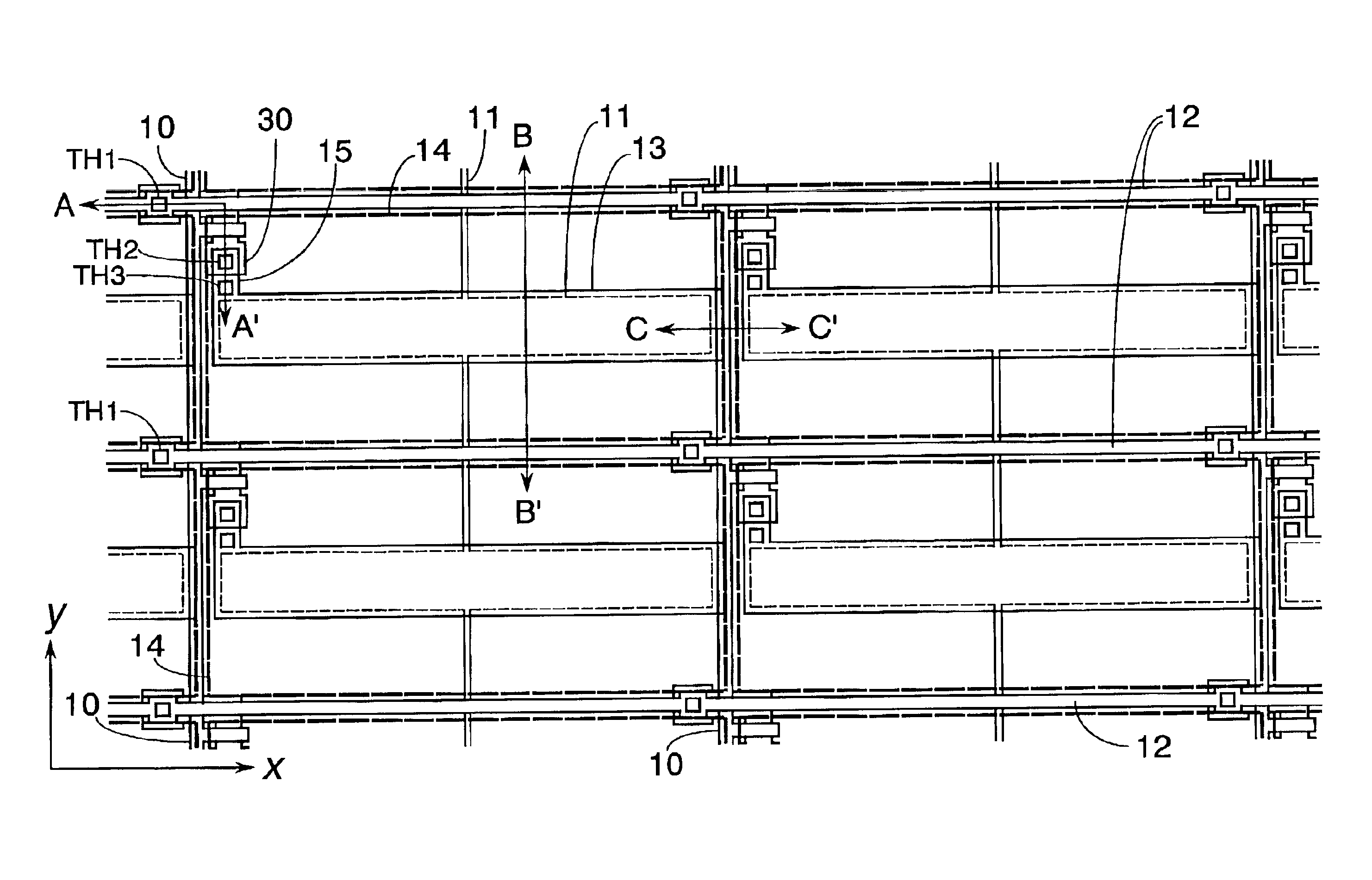
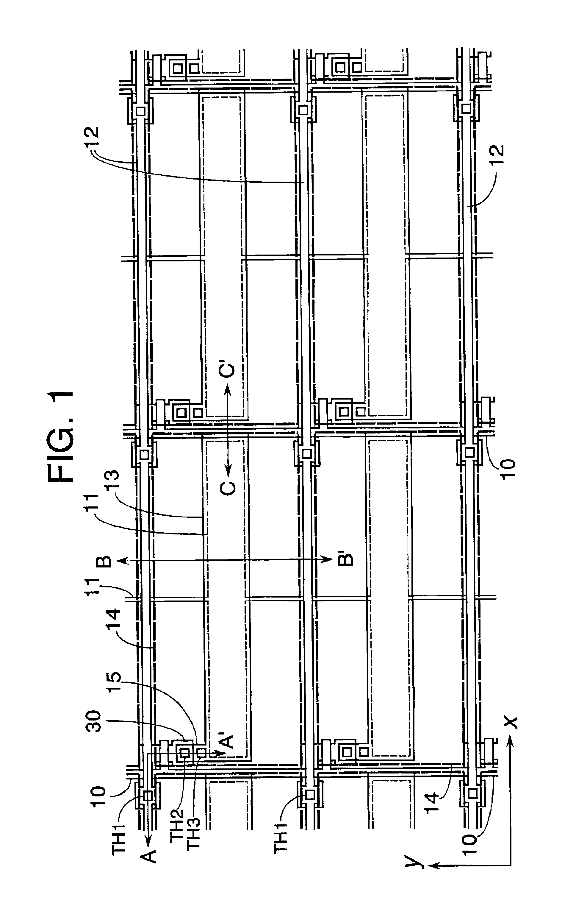
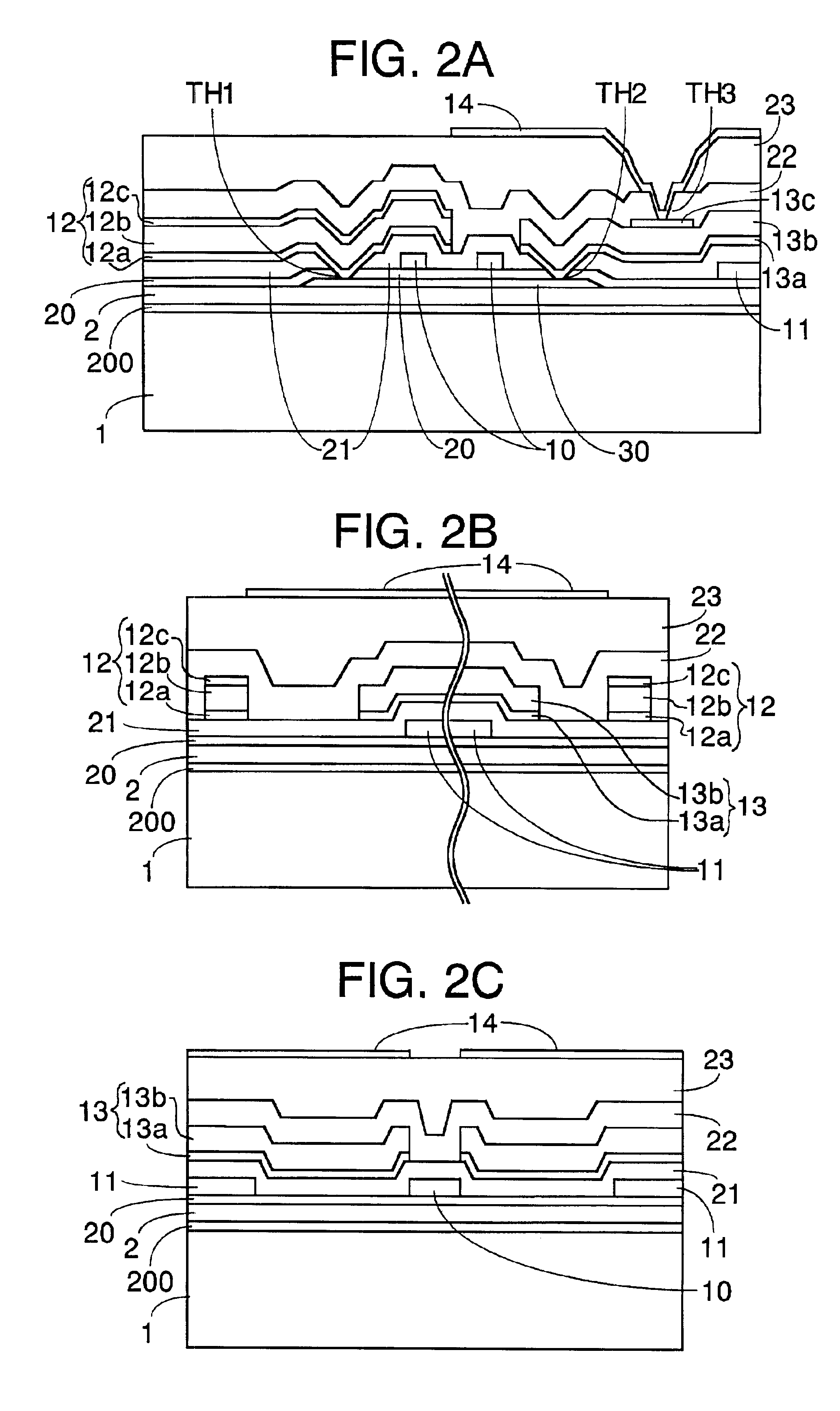
[0082]FIG. 1 is a diagram showing a plan view of a unitary picture element or “pixel” of a liquid crystal display device in accordance with the instant invention, and FIGS. 2A to 2C are diagrams each depicting a cross-sectional view of the pixel. FIGS. 2A to 2C illustrate sectional structures (i.e. sectional views resulted from cutaway along lines each having arrows at its both ends) as taken along lines A-A′, B-B′ and C-C′ of FIG. 1, respectively. Note here that the plan view of FIG. 1 (planar structures of pixel regions at four locations are shown so that these are disposed into an array) and each sectional view of FIGS. 2A to 2C illustrate only one substrate, called a TFT substrate, of a pair of substrates with a layer of liquid crystal material interposed therebetween, on which active elements (here, thin-film transistors or alternatively field effect transistors known as FETs) are formed for control of a display operation of each pixel, with the liquid crystal layer and the rem...

second embodiment

[0099]FIG. 3 and FIGS. 4A to 4C are diagrams showing a plan view and cross-sectional views of a unitary pixel of a liquid crystal display device in accordance with the present invention. FIGS. 4A to 4C show sectional structures taken along lines D-D′, E-E′ and F-F′ of FIG. 3, respectively. It should be noted that in a similar manner to FIGS. 1 and 2A to 2C, the plan view diagram of FIG. 3 and respective sectional views of FIGS. 4A to 4C only show the so-called TFT substrate of a pair of substrates of the liquid crystal display device with a liquid crystal layer sandwiched therebetween, wherein a polarizer plate or the like which is multilayered on a main surface on the opposite side to the liquid crystal layer in the sectional diagram of the TFT substrate is eliminated from the illustration.

[0100]It is formed on an insulating film for use as a buffer layer which is constituted from a Si3N4 film 200 with a film thickness of 50 nm and a SiO2 film 2 of 120 nm thick over a no-alkali gla...

third embodiment

[0107]FIG. 5 and FIGS. 6A to 6C are diagrams showing a plan view and cross-sectional views of a unitary pixel of a liquid crystal display device in accordance with the instant invention. FIGS. 6A to 6C show cross-sections of G-G′, H-H′ and I-I′ portions of FIG. 5, respectively. It should be noted that in a similar manner to FIGS. 1 and 2A to 2C, the plan view diagram of FIG. 5 and respective sectional views of FIG. 6A to 6C only show the so-called TFT substrate of a pair of substrates of the liquid crystal display device with a liquid crystal layer sandwiched therebetween, wherein a polarizer plate or the like to be multilayered on a main surface on the opposite side to the liquid crystal layer in the sectional diagram of the TFT substrate is eliminated from the illustration.

[0108]It is formed on an insulating film for use as a buffer layer which is constituted from a Si3N4 film 200 with a film thickness of 50 nm and a SiO2 film 2 of 120 nm thick over a no-alkali glass substrate 1 w...


PUM


Abstract

In a liquid crystal display device having a transmissive display region and a reflective display region within a unit pixel, the present invention disposes an optical reflection layer having an almost rectangular planar shape as extended in the unit pixel elongate direction at substantially a central portion midway between two neighboring signal electrodes, defines almost rectangular regions between the optical reflection layer and two signal electrodes adjacent thereto as the transmissive display region in the unit pixel, and forms a pixel electrode at a level spaced from that of the optical reflection layer by a dielectric film so as to cover the entire surface of the unit pixel, so that power consumption of the liquid crystal display device is reduced while image quality thereof is improved.

Description

BACKGROUND OF THE INVENTION[0001]1. Field of the Invention[0002]The present invention relates generally to liquid crystal display devices and, more particularly to the structure of a liquid crystal display device of the partial transmission and partial reflection type having both a transmissive display region and reflective display region.[0003]2. Description of the Related Art[0004]Owing to unique features such as thin or slim size, light weight and low power consumption, liquid crystal display devices are becoming more widely used as display devices for display of image and character information in a variety of types of electronic equipment including but not limited to information equipment such as personal computers, portable information terminals, mobile wireless telephone handsets, and visual equipment such as digital cameras and camera-embedded VTR apparatus and others. In recent years, in accordance with noticeable rapid popularization of mobile telephone handsets and handhel...

Claims


Application Information

Patent Timeline
IPC IPC(8): G02F1/1335G02F1/13G02F1/1362G02F1/1343G02F1/1368H01L21/77H01L27/12
CPCG02F1/133555H01L27/1214H01L27/12G02F1/136213G02F1/1335
Inventor KAWACHI, GENSHIROUMIYAZAWA, TOSHIONAGATA, TETSUYAHASEGAWA, ATSUSHI
Owner PANASONIC LIQUID CRYSTAL DISPLAY CO LTD
Why Eureka
Try Eureka