Display device, driving method for display device, and electronic apparatus

a technology of display device and driving method, which is applied in the direction of instruments, cathode-ray tube indicators, semiconductor devices, etc., can solve the problems of affecting the linearity of drain voltage-drain current characteristics, and affecting so as to reduce the variation of driving current for electrooptical elements caused by a kink phenomenon of driving transistors, the effect of improving the quality of display imag

Active Publication Date: 2010-06-10
JOLED INC
View PDF3 Cites 37 Cited by
  • Summary
  • Abstract
  • Description
  • Claims
  • Application Information

AI Technical Summary

Benefits of technology

[0018]It is desirable to provide a display device that reduces a variation in a driving current for an electrooptical element caused by a kink phenomenon of a driving transistor and thus improves the quality of a display image, a driving method for driving the display device, and an electronic apparatus including the display device.
[0020]When the power supply potential of the power supply line during the threshold correction period during which the threshold correction process is performed is the same as the power supply potential of the power supply line during the light-emission period for the electrooptical element, a difference occurs between the drain-source voltage Vds of the driving transistor after performance of the threshold correction process and the drain-source voltage Vds of the driving transistor during light emission of the electrooptical element. Thus, different potential values are set, as the power supply potential of the power supply line, for the threshold correction period and for the light-emission period. Hence, a difference between the drain-source voltage Vds after performance of the threshold correction process and the drain-source voltage Vds during light emission of the electrooptical element can be reduced compared with a case where the power supply potential of the power supply line during the threshold correction period is the same as the power supply potential of the power supply line during the light-emission period. As a result, even if a kink phenomenon occurs in the driving transistor and the degree of occurrence of the kink phenomenon varies in accordance with a manufacturing variation, a pixel-to-pixel variation in the drain-source current Ids of the driving transistor, furthermore, a variation in the driving current for the electrooptical element can be reduced.
[0021]According to an embodiment of the present invention, a variation in a driving current for an electrooptical element caused by a kink phenomenon of a driving transistor can be reduced. Thus, the quality of a display image can be improved.

Problems solved by technology

The kink phenomenon degrades the linearity of the drain voltage-drain current characteristics, and causes distortion of an output waveform.

Method used


Image

  • Display device, driving method for display device, and electronic apparatus
  • Display device, driving method for display device, and electronic apparatus
  • Display device, driving method for display device, and electronic apparatus

Examples


first embodiment

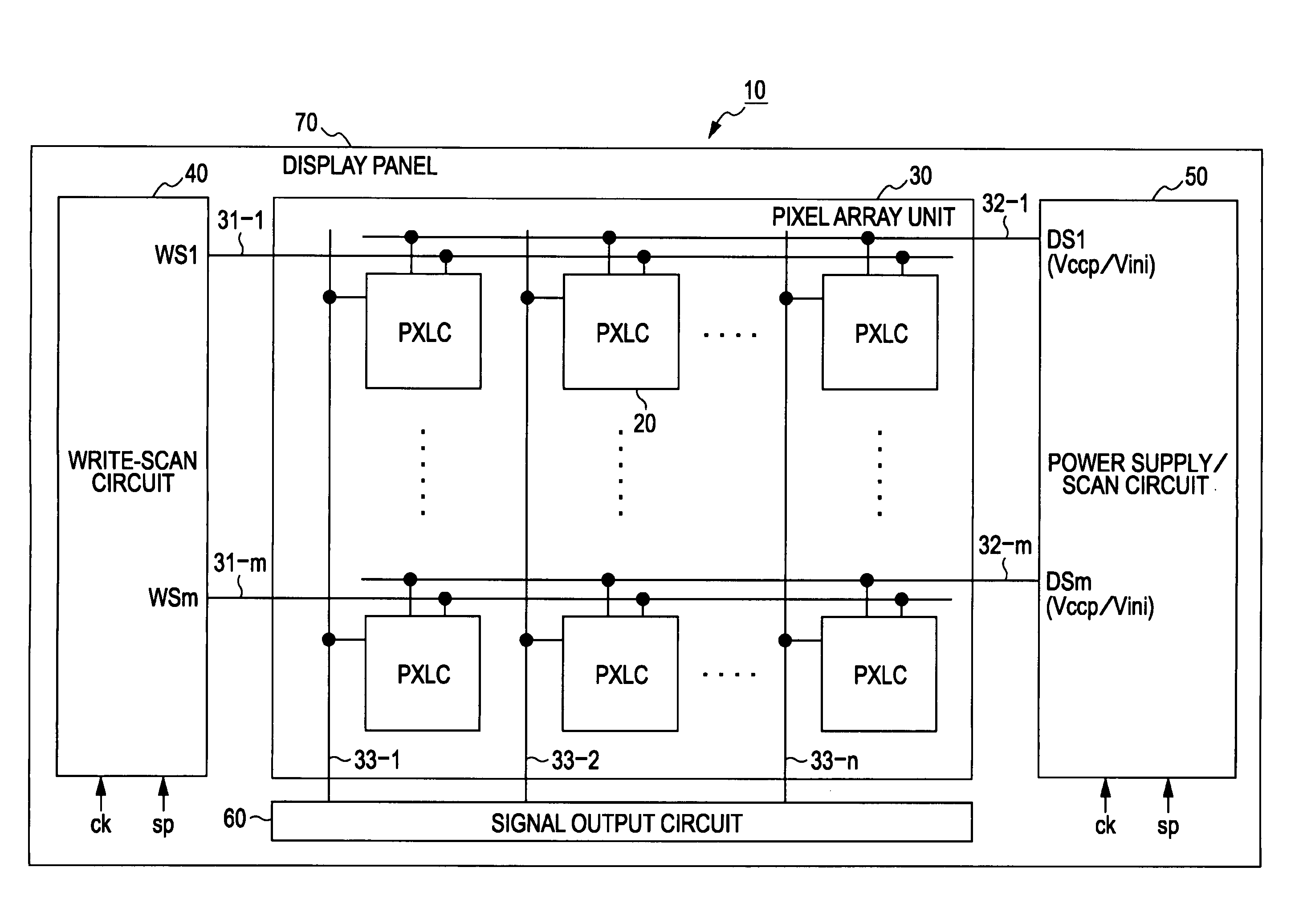
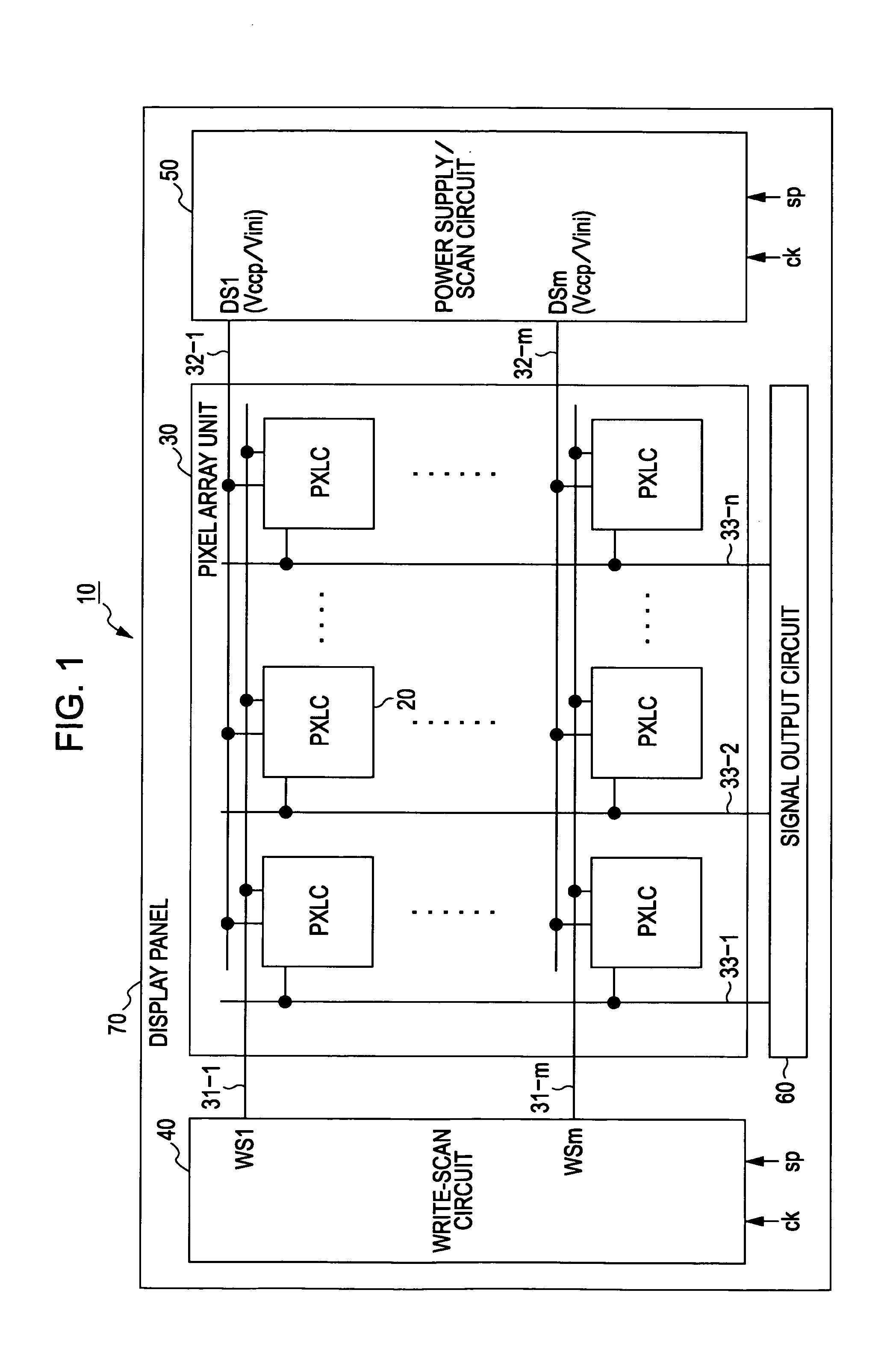
[0104]Organic EL display devices according to embodiments of the present invention are based on the organic EL display device 10 according to an embodiment of the present invention having the system configuration described above. An organic EL display device 10A according to a first embodiment of the present invention has a configuration in which the signal output circuit 60 selectively outputs the signal voltage Vsig of an image signal and the reference potential Vofs. As described above, the reference potential Vofs serves as a reference of the signal voltage Vsig of an image signal.

Circuit Operation

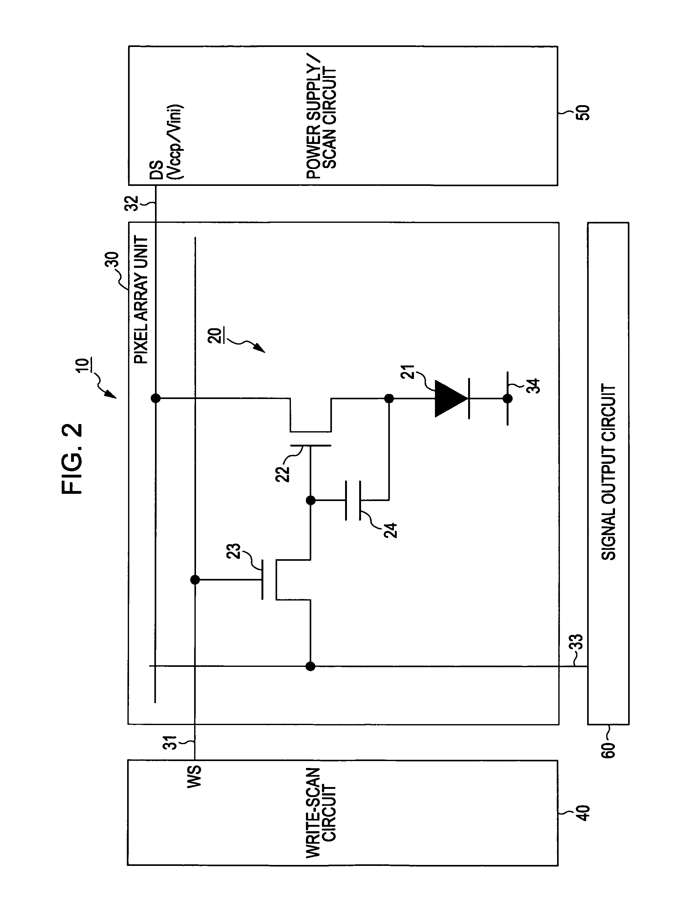
[0105]The basic circuit operation of the organic EL display device 10A according to the first embodiment will be described with reference to operation diagrams of FIGS. 5A to 5D and FIGS. 6A to 6D on the basis of a waveform timing chart of FIG. 4. For simplification, in the operation diagrams of FIGS. 5A to 5D and FIGS. 6A to 6D, the writing transistor 23 is illustrated by using a symb...

example 1

[0163]In the organic EL display device 10 having the system configuration shown in FIGS. 1 and 2, the power supply / scan circuit 50 according to Example 1 is configured to be capable of selectively setting three potential values as the potential DS of the power supply line 32. Specifically, the power supply / scan circuit 50 according to Example 1 is configured to be capable of selectively setting, in an appropriate manner, three potential values, the high potential Vccp (hereinafter, denoted by Vccp1), the low potential Vini, and an intermediate potential Vccp2 between the high potential Vccp (Vccp1) and the low potential Vini, as the power supply potential DS.

[0164]FIG. 13 illustrates a timing relationship regarding setting of the power supply potential DS according to Example 1. The power supply / scan circuit 50 sets the low potential Vini during a threshold correction preparation period (times t11 to t13), sets the intermediate potential Vccp2 at least during a threshold correction ...

example 2

[0181]In the organic EL display device 10 having the system configuration shown in FIGS. 1 and 2, the power supply / scan circuit 50 according to Example 2 is capable of selectively setting four potential values as the potential DS of the power supply line 32. Specifically, the power supply / scan circuit 50 is capable of selectively setting, in an appropriate manner, four potential values, the high potential Vccp1, the low potential Vini, and intermediate potentials Vccp2 and Vccp3 which are between the high potential Vccp1 and the low potential Vini. Here, the intermediate potentials Vccp2 and Vccp3 satisfy the relationship Vccp3.

[0182]In Example 1, the potential DS of the power supply line 32 during the mobility correction period (including the period for writing the signal voltage Vsig) is set to the intermediate potential Vccp2. That is, the potential DS of the power supply line 32 during the threshold correction period and the potential DS of the power supply line 32 during the mo...


PUM


Abstract

A display device includes a pixel array unit including pixels arranged in a matrix, the pixels each including an electrooptical element, a writing transistor for writing an image signal, a storage capacitor for storing the image signal, and a driving transistor for driving the electrooptical element in accordance with the image signal, the pixels each having a threshold correction process function for, before light emission of the electrooptical element, changing a source potential of the driving transistor to a potential obtained by subtracting a threshold voltage of the driving transistor from an initial gate potential of the driving transistor; and a power supply unit configured to set, as a power supply potential of a power supply line for supplying a current to the driving transistor, different potential values for a threshold correction period for execution of the threshold correction process and a light-emission period for the electrooptical element.

Description

BACKGROUND OF THE INVENTION[0001]1. Field of the Invention[0002]The present invention relates to display devices, driving methods for display devices, and electronic apparatuses, and more particularly, to a flat-screen (flat panel) display device in which pixels are two-dimensionally arranged in a matrix, a driving method for the display device, and an electronic apparatus including the display device.[0003]2. Description of the Related Art[0004]In recent years, in the area of display devices that display images, flat-screen display devices in which pixels (pixel circuits) are arranged in a matrix have rapidly become popular. Display devices including, as light-emitting elements of individual pixels, so-called current-driven electrooptical elements whose light emission luminances vary in accordance with the values of currents flowing in the elements, are one type of flat-screen display devices. In addition, organic electroluminescence (EL) elements exhibiting a phenomenon of emittin...

Claims


Application Information

Patent Timeline
Patent Type & Authority Applications(United States)
IPC IPC(8): G06F3/038
CPCG09G3/3233G09G2300/0819G09G2300/0842G09G2300/0866H01L2251/5315G09G2320/043G09G2330/028H01L27/3244H01L51/5221G09G2320/0219H10K59/12H10K50/824H10K50/828H10K2102/3026
Inventor TOMIDA, MASATSUGUASANO, MITSURU
Owner JOLED INC
Why Eureka
Try Eureka