Three-gate power LDMOS

A technology of power and the other side, applied in electrical components, circuits, semiconductor devices, etc., can solve the problems of small conduction area of ​​low-resistance channels, reduce channel resistance, reduce specific on-resistance, and increase doping concentration Effect

Active Publication Date: 2016-10-12
UNIV OF ELECTRONICS SCI & TECH OF CHINA
View PDF3 Cites 10 Cited by
  • Summary
  • Abstract
  • Description
  • Claims
  • Application Information

AI Technical Summary

Problems solved by technology

However, since the conduction area of ​​the low-resistance channel of ultra-thin SOI is still small, the specific on-resistance needs to be further improved.

Method used


Image

  • Three-gate power LDMOS
  • Three-gate power LDMOS
  • Three-gate power LDMOS

Examples


Embodiment 1

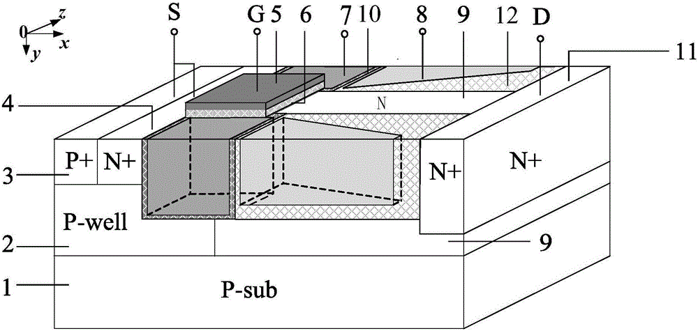
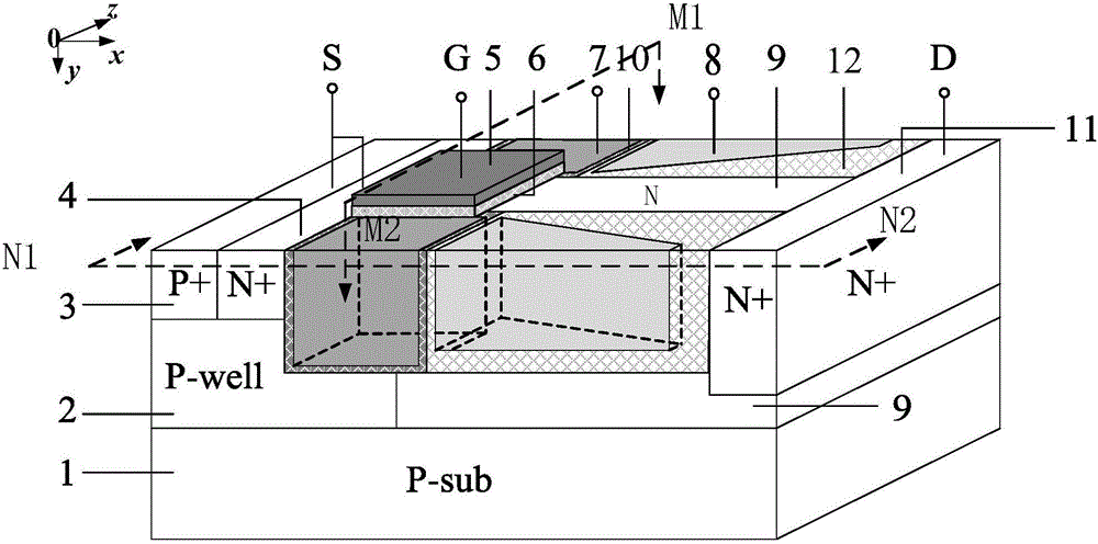
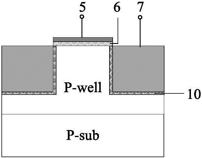
[0028] A tri-gate power LDMOS in this example, such as figure 1 As shown, a substrate layer 1 is included, one end of the upper surface of the substrate layer 1 has a P-type semiconductor body region 2, and the other end has an N-type semiconductor drift region 9, and the P-type semiconductor body region 2 and the N-type semiconductor drift region 9 contacts; the top of the P-type semiconductor body region 2 has a P-type semiconductor contact region 3 and an N-type semiconductor source region 4 on the side away from the N-type semiconductor drift region 9, and the N-type semiconductor source region 4 is located close to the N-type semiconductor drift region One side of 9; the upper surface of the P-type semiconductor body contact region 3 and the N-type semiconductor source region 4 is connected to the source metal; the N-type semiconductor drift region 9 has an N-type semiconductor drain region at one end away from the P-type semiconductor body region 2 11. The upper surface ...

Embodiment 2

[0031] Such as Figure 5 As shown, compared with Embodiment 1, the N-type semiconductor drift region 9 of this embodiment adopts a variable width. The semiconductor drift region 9 with variable width increases multiple sub-conduction paths, further reducing the on-resistance.

Embodiment 3

[0033] Such as Figure 6 As shown, compared with Embodiment 1, the drift region 9 of the N-type semiconductor in this embodiment is laterally doped, and its doping concentration gradually increases from the body region 2 to the N-type semiconductor drain region 11 . The linearly varying doping concentration modulates the electric field distribution in the drift region 9 of the N-type semiconductor, increasing the breakdown voltage.


PUM


Abstract

The invention belongs to the field of power semiconductor devices, and relates to a lateral three-gate power LDMOS based on a bulk silicon technology. The three-gate power LDMOS is mainly characterized by having a three-gate structure and a second conductive material electrically connected with a source or a gate or an external electrode. The three-gate power LDMOS has the main advantages that the three-gate structure increases the channel density and reduces the channel resistance, and thus, the specific on-resistance drops; the second conductive material can freely select the electrode, when the gate electrode is connected, in the positive case, electron accumulation surfaces are formed on the side surface and the bottom surface of a second groove, a multi-dimension low-resistance channel is formed, and the specific on-resistance is greatly reduced, and in the reverse case, assistant depletion of a drift region is carried out, the drift area doping concentration of the device is increased, the specific on-resistance of the device is reduced; when the source electrode is connected, gate-drain overlapping is reduced, the gate-drain capacitance of the device is reduced, and switching loss is reduced; and when the external electrode is electrically connected, multiple effects can be achieved.

Description

technical field [0001] The invention belongs to the field of lateral power semiconductor devices, and more precisely relates to a tri-gate power LDMOS based on bulk silicon technology. Background technique [0002] The key parameters of power LDMOS are withstand voltage and specific on-resistance. Improving the device withstand voltage requires increasing the length of the drift region and reducing its doping concentration, but this will cause the specific on-resistance to be R on,sp ∝BV 2.5 The form increases accordingly, this is the "silicon limit" problem that power LDMOS exists. [0003] In order to reduce the channel resistance, some researchers proposed a trench gate structure (A.Narazaki; Y.Hisamoto; C.Tadokoro; M.Takeda; H.Hagino [A novel 30V p-channel trench gate power MOSFET with ultra lowon-state- resistance at low-gate-voltage Power Semiconductor Devices and IC's], 1997.ISPSD'97.), the structure increases the channel density, broadens the carrier flow path, an...

Claims


Application Information

Patent Timeline
Patent Type & Authority Applications(China)
IPC IPC(8): H01L29/78
CPCH01L29/7816H01L29/7831H01L29/063H01L29/0653H01L29/0847H01L29/0878H01L29/0882H01L29/0886H01L29/404H01L29/407H01L29/7825H01L29/7835H01L29/785H01L29/0696H01L29/4238
Inventor 罗小蓉葛薇薇吴俊峰马达吕孟山黄琳华刘庆孙涛
Owner UNIV OF ELECTRONICS SCI & TECH OF CHINA
Why Eureka
Try Eureka