Method for manufacturing circuit board by addition method

An additive and circuit technology, applied in the direction of conductive pattern formation, etc., can solve the problems of difficult etching, etching of base copper foil, side etching of lines, etc., to achieve the effect of cost and environmental advantages

Inactive Publication Date: 2012-10-03
凯迪思科技股份有限公司 +1
View PDF3 Cites 24 Cited by
  • Summary
  • Abstract
  • Description
  • Claims
  • Application Information

AI Technical Summary

Problems solved by technology

[0006] The process of the semi-additive method and the subtractive method is simple and the process is mature, but there will be etching of the base copper foil, which will cause side etching of the circuit. For ultra-thin lines and ultra-thick copper foil, the two processes have inherent Generally speaking, it is very difficult to make a line width and spacing less than 4mil, and it is difficult to etch a copper thickness greater than 4OZ.

Method used


Image

  • Method for manufacturing circuit board by addition method
  • Method for manufacturing circuit board by addition method

Examples


Embodiment Construction

[0017] In order to illustrate the specific implementation method of the present invention, the present invention will be further described in detail below in conjunction with the accompanying drawings.

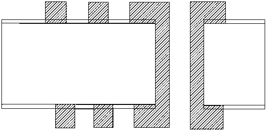
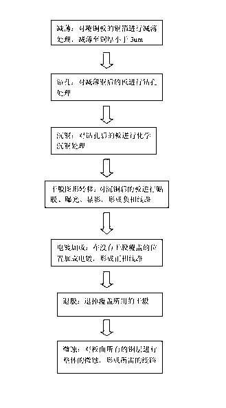
[0018] The process of the invention is: thinning→drilling→copper sinking→dry film pattern transfer→electroplating addition→film removal→microetching.

[0019] Thinning: The copper foil of the copper clad laminate is thinned until the copper thickness is less than 3um. The thinner the initial thickness of the copper foil, the better. Generally, a copper thickness of 18um is used. The adjustment is based on the etching speed of the 18um copper foil in the inner layer, which is twice the etching rate of the inner layer, and the remaining thickness of the copper foil is less than 3um and the base material is slightly exposed.

[0020] Drilling: Drilling is performed on the thinned copper board. Before the thinning is drilled, it is to avoid etching the inner layer of the multilay...


PUM


Abstract

The invention provides a method for manufacturing a circuit board by an addition method. The process is as follows: thinning, drilling; precipitating copper; transferring a dry film image; and conducting electroplating addition, film withdrawing and microetching. By adopting the circuit board manufactured by adopting the method, the line width / interval being smaller than 4mil / 4mil can be realized easily, a circuit board with ultra-thick copper can be manufactured, and the quality problems of blocked holes and line breakage can be reduced greatly.

Description

technical field [0001] The invention belongs to the technical field of printed circuit board production, and specifically relates to a method for producing circuit boards by an additive method. Background technique [0002] At present, there are generally only two methods for making circuit boards, the semi-additive method and the subtractive method for making circuit boards. [0003] The method of making circuit boards by pattern electroplating process is a semi-additive method. This method is based on the base copper foil for chemical copper, thickened copper plating, dry film pattern transfer, pattern electroplating, secondary thickened copper plating, and tin plating. The process flow of lead, film stripping, etching, and stripping tin is used to make circuit boards. [0004] The method of using the dry film masking process to make circuit boards is the subtractive method. This method is based on the base copper foil, which is based on the process of chemical copper, on...

Claims


Application Information

Patent Timeline
Patent Type & Authority Applications(China)
IPC IPC(8): H05K3/10
Inventor 黄明安
Owner 凯迪思科技股份有限公司
Why Eureka
Try Eureka