Supercharge Your Innovation With Domain-Expert AI Agents!

Light-emitting diode (LED) packaging body and manufacturing method thereof as well as LED

An LED package and LED chip technology, which is applied to semiconductor devices, electrical components, circuits, etc., can solve the problems of easy contamination of circuit boards and poor stability of LED packages, and achieve stable connection, strong stability, and avoidance of pollution. Effect

Active Publication Date: 2015-04-29
SHENZHEN SUNSCREEN CO LTD +1
View PDF3 Cites 0 Cited by
  • Summary
  • Abstract
  • Description
  • Claims
  • Application Information

AI Technical Summary

Problems solved by technology

[0003] The purpose of the present invention is to provide a method for manufacturing an LED package, aiming to solve the problems of the prior art that the circuit board of the LED package is easily polluted and the stability of the LED package is poor

Method used


Image

  • Light-emitting diode (LED) packaging body and manufacturing method thereof as well as LED
  • Light-emitting diode (LED) packaging body and manufacturing method thereof as well as LED
  • Light-emitting diode (LED) packaging body and manufacturing method thereof as well as LED

Examples


Embodiment Construction

[0026] In order to make the object, technical solution and advantages of the present invention clearer, the present invention will be further described in detail below in conjunction with the accompanying drawings and embodiments. It should be understood that the specific embodiments described here are only used to explain the present invention, not to limit the present invention.

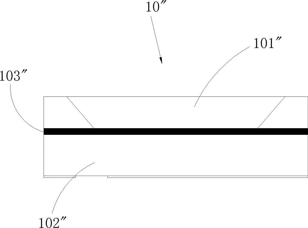
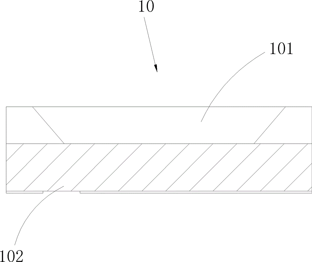
[0027] The invention provides a method for manufacturing an LED package, comprising the following steps:

[0028] (1) Place the circuit board provided with electrodes on the mold core of the high temperature molding machine;

[0029] (2) Inject high-temperature resin into the mold core of the high-temperature molding press, so that the high-temperature resin is in contact with the circuit board;

[0030] (3) The high-temperature resin forms a housing on the circuit board with a through cavity and one end is directly attached to the circuit board;

[0031] (4) After the high-temperature resin is f...


PUM


Abstract

The invention relates to the technical field of light-emitting diodes (LED), and discloses an LED packaging body and a manufacturing method thereof as well as an LED. The manufacturing method comprises the following steps of: (1) placing a circuit board on a mould core of a high-temperature moulding press; (2) injecting high-temperature resin into the high-temperature moulding press to ensure that the high-temperature resin is combined with the circuit board in a contact mode; (3) forming a shell on the circuit board by using the high-temperature resin, wherein the shell is provided with a through cavity and one end of the shell is directly attached to the circuit board; (4) forming the LED packaging body by the circuit board and the shell; and (5) separating the shell from the mould core, and taking the LED packaging body out of the high-temperature moulding press. Compared with the prior art, an adhesive glue is not required to be arranged between the shell and the circuit board, so that the phenomenon that the circuit board is polluted is avoided, and the LED packaging body manufactured by the method is strong in stability, and the connection between the circuit board and the shell is firm.

Description

technical field [0001] The invention relates to the technical field of LEDs, in particular to an LED packaging body, a manufacturing method thereof, and an LED. Background technique [0002] In the existing technology, such as figure 1 As shown, the LED package 10" includes a circuit board 102" and a housing 101" attached to the top of the circuit board 102", and the housing 101" is generally attached to the top of the circuit board 102" through an adhesive 103". Like this, in the process of carrying out housing 101 " and circuit board 102 " bonding, adhesive glue 103 " can overflow because of the extruding of housing 101 " and circuit board 102 ", thereby, pollute circuit board 102 " easily, Moreover, the stability of the LED package 10 ″ bonded in this way is relatively poor, that is, the adhesion between the circuit board 102 ″ and the housing 101 ″ is not stable enough, especially when the LED package 10 ″ is subjected to post-processing. During the process of forming ...

Claims


Application Information

Patent Timeline
Patent Type & Authority Patents(China)
IPC IPC(8): H01L33/00H01L33/54
Inventor 宋文洲
Owner SHENZHEN SUNSCREEN CO LTD
Features
  • R&D
  • Intellectual Property
  • Life Sciences
  • Materials
  • Tech Scout
  • Unparalleled Data Quality
  • Higher Quality Content
  • 60% Fewer Hallucinations
Learn More