Metal-oxide-semiconductor field-effect transistor layout structure

A technology of metal oxide half-field and layout structure, which is applied in the direction of semiconductor devices, electrical components, circuits, etc., and can solve problems such as asymmetry of online circuits

Inactive Publication Date: 2012-10-31
INTEGRATED SYST SOLUTION
View PDF4 Cites 0 Cited by
  • Summary
  • Abstract
  • Description
  • Claims
  • Application Information

AI Technical Summary

Problems solved by technology

Generally speaking, it has (1) whether the corners of the source 120 and the

Method used


Image

  • Metal-oxide-semiconductor field-effect transistor layout structure
  • Metal-oxide-semiconductor field-effect transistor layout structure
  • Metal-oxide-semiconductor field-effect transistor layout structure

Examples


Embodiment Construction

[0036] Although the present invention may be embodied in different forms, what is shown in the drawings and described below is a preferred embodiment of the invention, and it is to be understood that what is disclosed herein is considered an example of the invention , and are not intended to limit the invention to the particular embodiments shown and / or described.

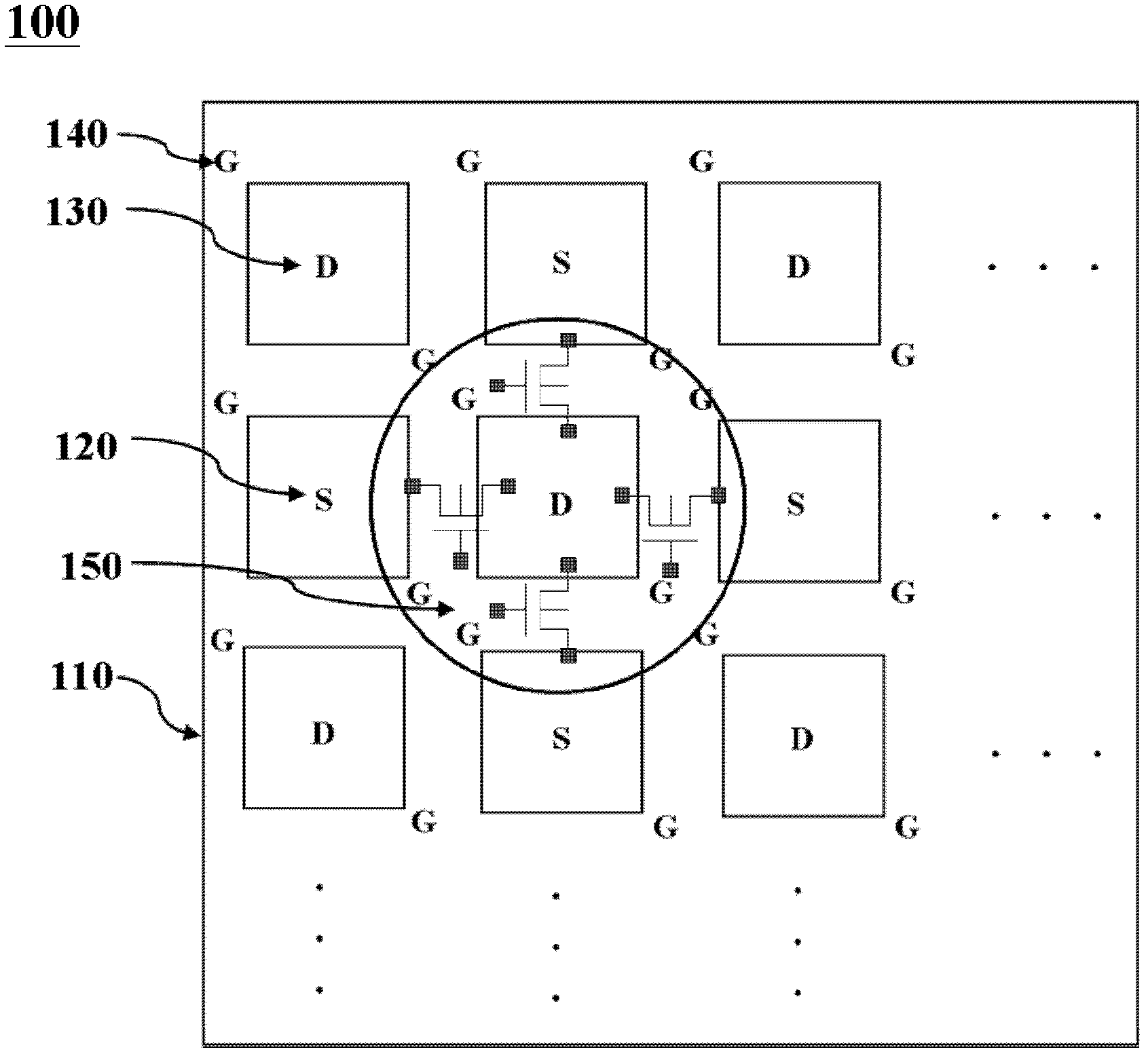
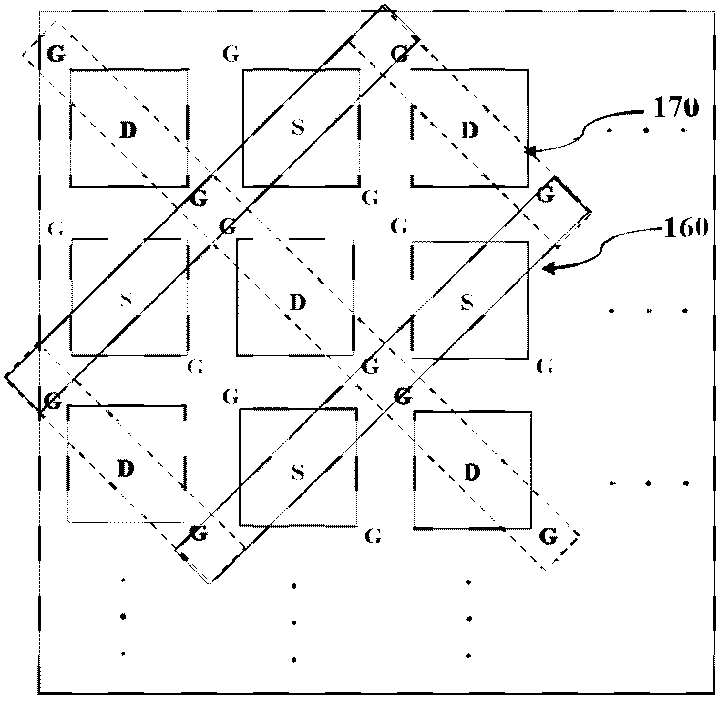
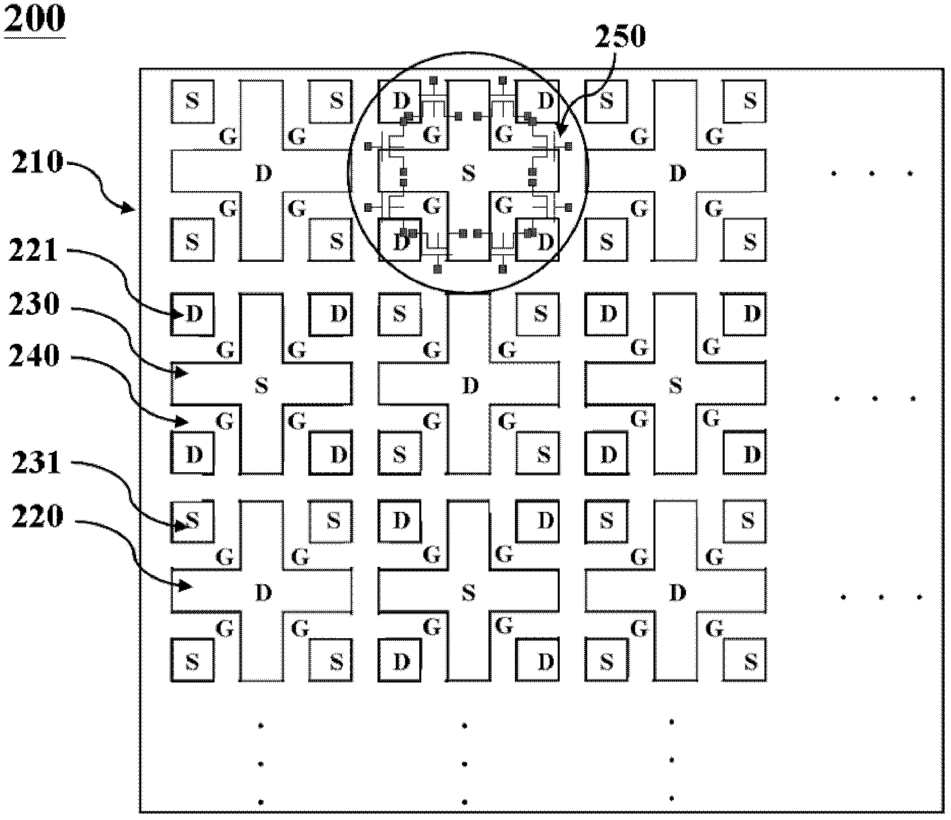
[0037] Please refer now Figure 2A , which shows a schematic diagram of the layout structure of a metal-oxide-semiconductor field-effect transistor with a higher effective channel width and a higher component density in the present invention. It includes: a substrate; a common drain region 220 with a cross pattern; at least two common source regions 231 with a grid pattern; a common source region 230 with a cross pattern; at least two common source regions 231 with a grid pattern a common drain region 221 ; and at least two common gate regions 240 . A common drain region 220 with a cross pattern is formed on the ...


PUM


Abstract

Disclosed is a metal-oxide-semiconductor field-effect transistor layout structure, which employs a common drain area having a right cross-shaped pattern and at least two common drain areas having tartan design, and a mixed array having a right cross-shaped pattern common drain area and a right cross-shaped pattern common source electrode which are formed by a common source electrode area having a right cross-shaped pattern and at least two common source electrode areas having tartan design. The metal-oxide-semiconductor field-effect transistor layout structure can improve the assembly density of the conventional layout circuit and promote the width of the efficient information channel thereof, thereby realizing the objective of reducing the cost and operation with higher power.

Description

technical field [0001] The invention relates to a layout structure of a metal oxide half field effect transistor, in particular to a layout structure of a metal oxide half field effect transistor with a higher effective channel width and a higher component density, which can increase the component density of a traditional layout circuit and improve its Effective channel width for lower cost and higher power operation. Background technique [0002] In recent years, Metal Oxide Semiconductor (MOS) has achieved the purpose of increasing device speed and driving current by reducing the size of the device. near the limit. Therefore, it is becoming more and more difficult to achieve performance improvement by reducing the size of components. [0003] In addition, Metal Oxide Semiconductor Field Effect Transistors (Power MOS) with large line widths are also widely used as power switches for power management applications. However, the excessively long connecting wires of the sour...

Claims


Application Information

Patent Timeline
IPC IPC(8): H01L29/78H01L29/08
Inventor 庄家硕赖宜贤吴美珍
Owner INTEGRATED SYST SOLUTION
Why Eureka
Try Eureka