Integration of metal-oxide-semiconductor field-effect transistor (MOSFET) and Schottky diode and method for manufacturing same

A technology of Schottky diodes and field effect transistors, which is applied in the field of integration and production of metal oxide semiconductor field effect transistors and Schottky diodes, can solve the problems of film layer production and strict control, so as to increase component density and improve The effect of pressure resistance

Inactive Publication Date: 2012-02-01
ANPEC ELECTRONICS CORPORATION
View PDF4 Cites 4 Cited by
  • Summary
  • Abstract
  • Description
  • Claims
  • Application Information

AI Technical Summary

Problems solved by technology

[0004] Although TMBS can achieve the goal of integrating Mosfet 110 and Schottky diode 120, the trenches 104a, 104b and the dielectric layer need 112, conductive layer 114 and other film production and control are increasingly strict; in addition, it is necessary to consider the production and control of TMBS and other high-density processes such as tungsten processes

Method used


Image

  • Integration of metal-oxide-semiconductor field-effect transistor (MOSFET) and Schottky diode and method for manufacturing same
  • Integration of metal-oxide-semiconductor field-effect transistor (MOSFET) and Schottky diode and method for manufacturing same
  • Integration of metal-oxide-semiconductor field-effect transistor (MOSFET) and Schottky diode and method for manufacturing same

Examples


Embodiment Construction

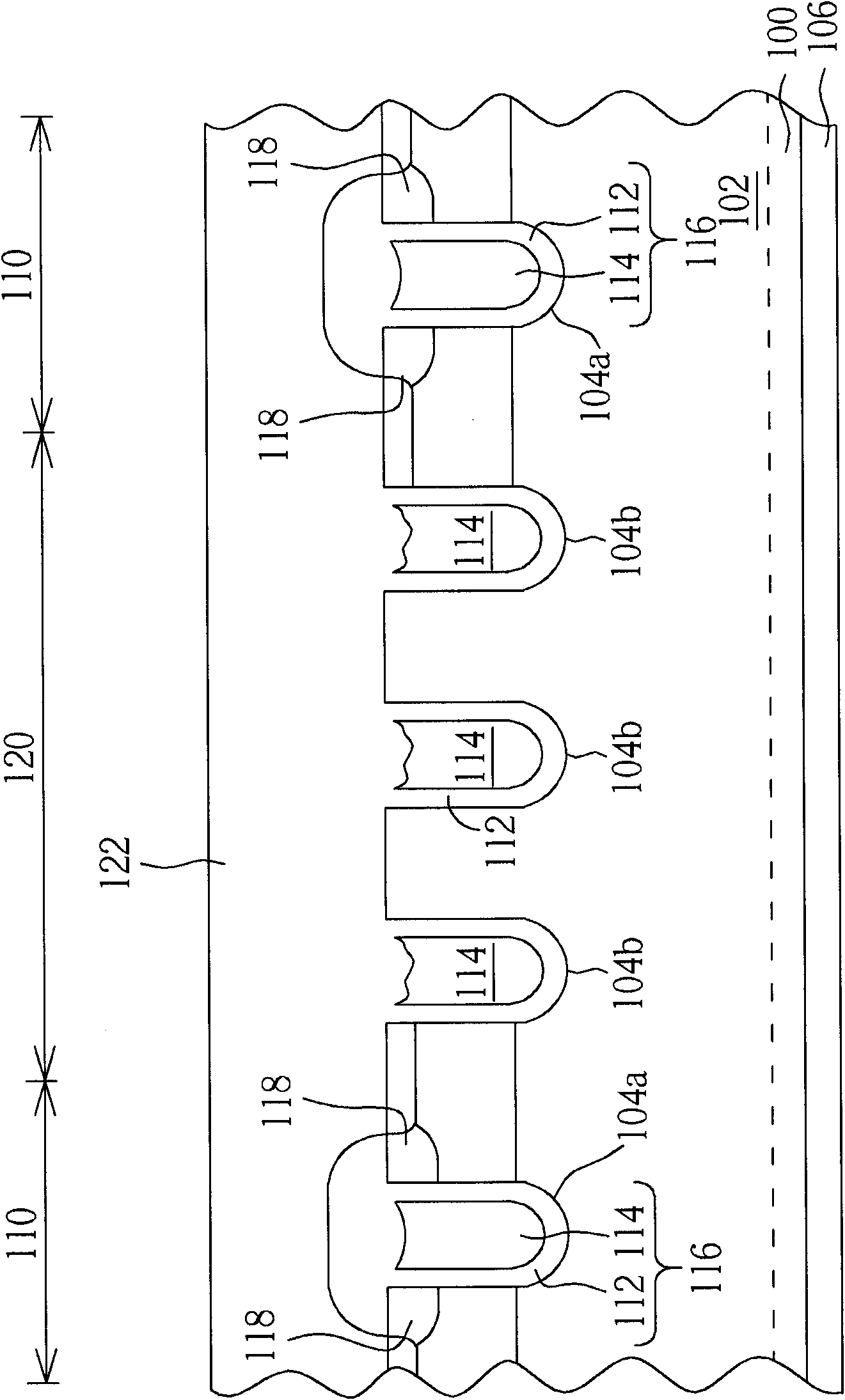
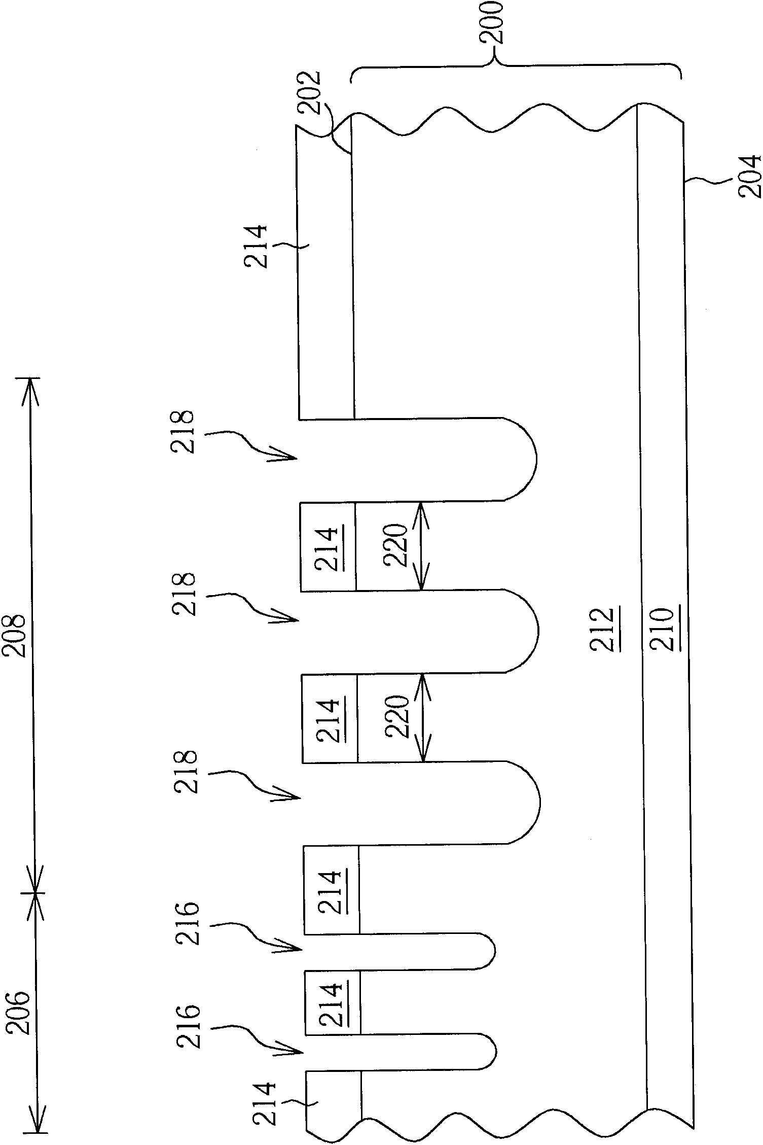
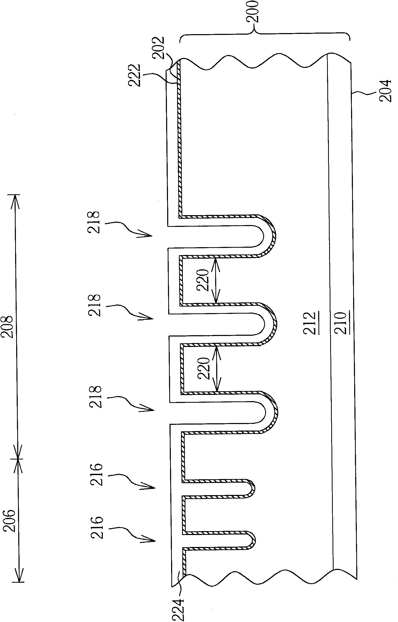
[0034] see Figure 2 to Figure 10 . Figure 2 to Figure 10 It is a schematic diagram of a first preferred embodiment of the manufacturing method of the metal oxide semiconductor field effect transistor and Schottky diode integrated assembly provided by the present invention. Such as figure 2 As shown, firstly a semiconductor substrate 200 is provided, the semiconductor substrate 200 includes a first surface 202 and an opposite second surface 204, and the first surface 202 defines at least one metal oxide semiconductor field effect transistor region 206 and a Schottky base diode region 208 . The semiconductor substrate 200 includes a silicon substrate 210 and an epitaxial silicon layer 212 formed on the silicon substrate 210 . Both the silicon substrate 210 and the epitaxial silicon layer 212 have a first doping type, and in this preferred embodiment, the first doping type is N type; and the silicon substrate 210 is heavily doped, that is, its doping concentration is higher...


PUM

PropertyMeasurementUnit
Thicknessaaaaaaaaaa
Thicknessaaaaaaaaaa

Abstract

The invention discloses an integrated component of a metal-oxide-semiconductor field-effect transistor (MOSFET) and a Schottky diode. The component comprises a semiconductor substrate, a plurality of first trenches and a plurality of second trenches, wherein the semiconductor substrate is used for defining an MOSFET area and a Schottky diode area; the first trenches are arranged in the MOSFET area; and the second trenches are arranged in the Schottky diode area. The first trenches comprise a first insulating layer and a first conductive layer, wherein the first insulating layer is used for covering the bottom and the side wall of the first trenches, and the first conductive layer is used for serving as a trenched gate of a trench MOSFET. Both the width and the depth of the second trenchesare more than that of the first trenches, and the second trenches respectively comprise a second insulating layer and a second conductive layer, wherein the second insulating layer is used for covering the bottom and the side wall of the second trenches, and the thickness of second conductive layer is more than that of the first insulating layer.

Description

technical field [0001] The present invention relates to a semiconductor component integrating a Metal-Oxide-Semiconductor Field-Effect Transistor (MOSET) and a Schottky diode and a manufacturing method thereof, especially to an integrated trench-type metal-oxide-semiconductor A semiconductor component of a transistor component and a Schottky diode (trench MOS barrier Schottky, TMBS) and a manufacturing method thereof. Background technique [0002] Schottky diode components are diode components composed of metal and semiconductor junctions, like general PN junction diodes, which have unidirectional conduction characteristics. And because the Schottky diode is unipolar, its start-up voltage is lower than that of the PN diode component, and the reaction speed is faster when switching forward and reverse biases, so it is especially used to reduce power consumption and improve switching. Speed, and widely used in power conversion circuits (power converter). For example, the int...

Claims


Application Information

Patent Timeline
IPC IPC(8): H01L27/04H01L29/06H01L21/77
CPCH01L29/8725H01L29/66143
Inventor 林伟捷林礼政徐信佑陈和泰叶人豪杨国良陈佳慧洪世杰
Owner ANPEC ELECTRONICS CORPORATION
Why Eureka
Try Eureka