Supercharge Your Innovation With Domain-Expert AI Agents!

Defect detecting method for utilizing graphic features to scan and manufacturing method of semiconductor chip

A defect detection and pattern feature technology, applied in the direction of semiconductor/solid state device testing/measurement, etc., can solve the problem of not being able to detect the chip and so on

Inactive Publication Date: 2012-11-21
SHANGHAI HUALI MICROELECTRONICS CORP
View PDF5 Cites 14 Cited by
  • Summary
  • Abstract
  • Description
  • Claims
  • Application Information

AI Technical Summary

Problems solved by technology

[0004] However, since regular repeating devices such as memories are repeating units in physical structure, as shown in the figure above, A and B are two identical minimum memory repeating units, and the places indicated by the arrows on the figure are defective position, but there are defects at the same position of each repeat unit, and this problem on the chip cannot be detected by existing detection methods (that is, "the same defect exists at the same position of each repeat unit " this question)

Method used


Image

  • Defect detecting method for utilizing graphic features to scan and manufacturing method of semiconductor chip
  • Defect detecting method for utilizing graphic features to scan and manufacturing method of semiconductor chip
  • Defect detecting method for utilizing graphic features to scan and manufacturing method of semiconductor chip

Examples


Embodiment Construction

[0023] In order to make the content of the present invention clearer and easier to understand, the content of the present invention will be described in detail below in conjunction with specific embodiments and accompanying drawings.

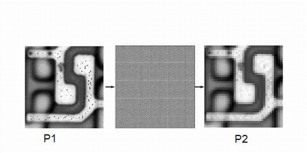
[0024] The inventors of the present invention have advantageously found that since regularly repeating semiconductor devices such as memories are all repeating units in physical structure, the smallest structure with periodic repetition can be obtained in the memory area of ​​the chip during defect detection, Therefore, the position of the defect can be found by comparing the data in the horizontal or vertical direction by repeating the structure.

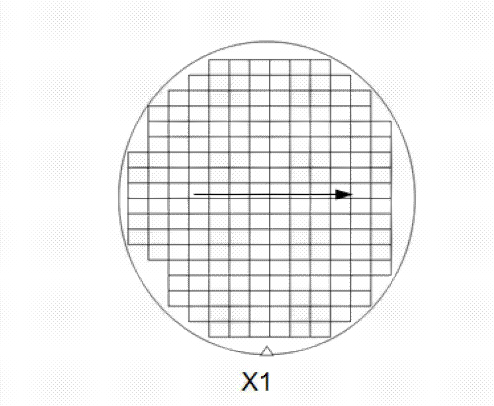
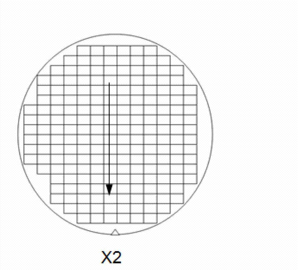
[0025] The technical principle of the present invention is to define repeating units cell1, cell2, cell3 and cell4 of semiconductor devices such as memory on the layout file of the chip through a terminal, such as Figure 5 Then import this file (repeating unit) into the defect detection program, the...


PUM


Abstract

The invention provides a defect detecting method for utilizing graphic features to scan and a manufacturing method of a semiconductor chip. The defect detecting method for utilizing graphic features to scan according to the invention comprises the following steps: 1) defining a repeated unit structure according to a semiconductor structure; 2) inputting a data graph of the repeated unit structure defined in the step 1) to a defect detecting program; 3) inputting a physical repeated structure of the semiconductor structure on the chip to the defect detecting program; 4) comparing the graphic features of the physical repeated structure and the data graph in the defect detecting program; and 5) detecting a defect position according to the compared difference from the step 4). The invention provides a high-precision and high-flexibility defect detecting method for detecting the defects in a same position on the repeated unit structure, such as a memory.

Description

technical field [0001] The present invention relates to the field of semiconductor manufacturing, more specifically, the present invention relates to a defect detection method utilizing pattern feature scanning, and in addition, the present invention also relates to a semiconductor chip manufacturing method employing the defect detection method utilizing pattern feature scanning . Background technique [0002] With the continuous improvement of integrated circuit technology, the number of devices per unit area of ​​the chip is also increasing, especially the semiconductor area such as the memory area is the place with the highest integration of devices on the chip, so the subtleties of the device structure Any change will lead to the failure of the final electrical performance. [0003] In order to be able to detect problems in time during the production process and take corresponding measures, a certain number of optical and electronic defect detection equipment will be eq...

Claims


Application Information

Patent Timeline
Patent Type & Authority Applications(China)
IPC IPC(8): H01L21/66
Inventor 倪棋梁陈宏璘龙吟郭明升
Owner SHANGHAI HUALI MICROELECTRONICS CORP
Features
  • R&D
  • Intellectual Property
  • Life Sciences
  • Materials
  • Tech Scout
  • Unparalleled Data Quality
  • Higher Quality Content
  • 60% Fewer Hallucinations
Learn More