Method for solving antenna effect in chip design

An antenna effect and chip design technology, applied to electrical components, electrical solid devices, circuits, etc., can solve problems such as area consumption, and achieve the effect of reducing area and consumption

Inactive Publication Date: 2012-11-28
BEIJING CEC HUADA ELECTRONIC DESIGN CO LTD
View PDF4 Cites 7 Cited by
  • Summary
  • Abstract
  • Description
  • Claims
  • Application Information

AI Technical Summary

Problems solved by technology

[0013] It can be seen from the above analysis results that if this method is adopted, it is necessa

Method used


Image

  • Method for solving antenna effect in chip design
  • Method for solving antenna effect in chip design

Examples


Embodiment Construction

[0018] In order to make the purpose, technical solutions and advantages of the embodiments of the present invention clearer, the implementation of the present invention will be further described in detail below in conjunction with the accompanying drawings. Here, the exemplary embodiments and descriptions of the present invention are used to explain the present invention, but not to limit the present invention.

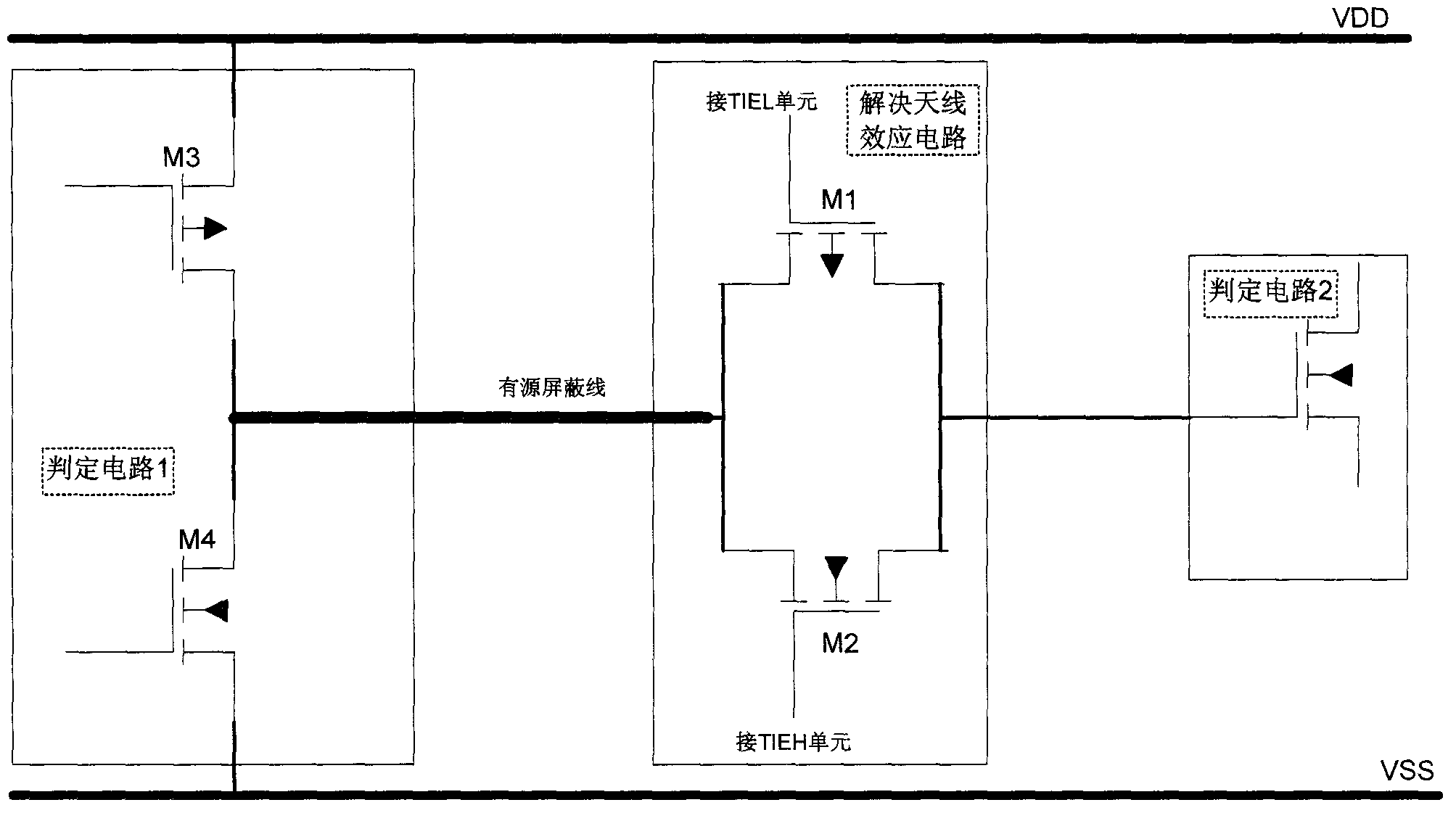
[0019] Such as figure 1 As shown, it is a frame diagram of the overall structure of the implementation method of the present invention. This embodiment includes (but not limited to) four functional modules: a judgment circuit 1, an active shielded wire, a circuit for solving antenna effects, and a judgment circuit 2.

[0020] Such as figure 1 Shown is a schematic diagram of the embodiment of the method and circuit for solving the antenna effect of the present invention, the circuit includes (but not limited to) a transmission gate circuit composed of PMOS and NMOS, a...


PUM


Abstract

The invention relates to a method and a circuit for solving the problem of antenna effect in a chip design. In some chip designs, an active shield physical protection design needs to be adopted for the purpose of preventing invasive attack to smart card chips. An active shielding layer has a defending effect on both attacks needing physical modification and those damaging partial functions of the chips. An active shielding line adopts a top layer metal and has a relatively long routing, and thus can cause severe antenna effect. When the traditional method of adding a diode is adopted, a relatively large chip area are usually occupied. The method provided by the method adopts a circuit with a transmission gate structure to solve the problem of antenna effect, and the circuit is simple in structure and easy to implement, and by using the method and the circuit, functions of the circuit are not affected.

Description

technical field [0001] The invention proposes a method and a circuit for solving the antenna effect in chip design. The invention is applicable to the field of smart card design. Background technique [0002] There are many attack methods against smart card chips, which can be roughly divided into three categories. Intrusive attack is one of them, also known as physical attack. Commonly used tools in chip reverse engineering include removing chip packages, extracting layouts, and cutting / connecting circuits. The active shielding layer has a defensive effect on attacks that require physical modification and destroy some functions of the chip. [0003] In the physical layout design of the smart card chip, the top layer metal is often used as the active shielding of the entire chip. Assume that the metal wires in the design start random routing at a certain starting point on the top layer, and cover the top layer of metal, and then connect to the standard unit through the lo...

Claims


Application Information

Patent Timeline
IPC IPC(8): H01L27/02
Inventor 李勇潘亮陈波涛
Owner BEIJING CEC HUADA ELECTRONIC DESIGN CO LTD
Why Eureka
Try Eureka