Memory compatible method

A technology of memory and non-volatile flash memory, which is applied in the direction of assembling printed circuits with electrical components, and can solve problems that do not involve the technical characteristics of memory

Active Publication Date: 2015-04-08
宁波麦度智联科技股份有限公司
View PDF7 Cites 1 Cited by
  • Summary
  • Abstract
  • Description
  • Claims
  • Application Information

AI Technical Summary

Problems solved by technology

[0006] Neither of the above two patents involves the technical features of memory compatibility by pasting stencils on the pads

Method used


Image

  • Memory compatible method
  • Memory compatible method
  • Memory compatible method

Examples


Embodiment Construction

[0024] The present invention will be further described below in conjunction with the accompanying drawings and specific embodiments, but not as a limitation of the present invention.

[0025] In the field of semiconductors, the compatibility of memory NAND and EMMC can save costs, and has high versatility. All kinds of electronic products can be used, which is simple and convenient, and improves the market competitiveness of electronic products.

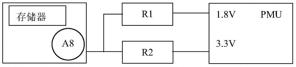
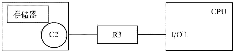
[0026] Therefore, the present invention designs a way to realize the compatibility of the above two memories. Originally, the two memories are connected to the CPU by adding an additional control circuit. Control the short connection and isolation between the pads by means of a method, which not only achieves the function of the original circuit, but also realizes the reduction of the functional area of ​​the device and improves the performance of the product.

[0027] Such as image 3 , Figure 4 , Figure 5 As shown, the present...


PUM


Abstract

The invention relates to a memory compatible method which comprises the following steps: firstly providing a PCB (Printed Circuit Board) provided with a first bonding pad and a second bonding pad, wherein a set distance exists between the first bonding pad and the second bonding pad; performing green oil windowing on the first bonding pad and the second bonding pad; when the first bonding pad and the second bonding pad need signal connection, designing steel mesh windowing according to the PCB and the bonding pads; printing a tin paste on the bonding pads by use of a steel mesh printing process and electrically connecting the first bonding pad and the second bonding pad by use of a fluid welding furnace; when electric connection is not needed, enabling the PCB subjected to first bonding pad and second bonding pad green oil windowing to directly pass through the fluid welding furnace. By virtue of such a design, the wiring space is effectively reduced and the production cost is lowered; an original resistor circuit is replaced by such combination, so that a main board area is reduced; under the condition that the main board size is constant, other electronic components can be installed on the saved area, and the product performance is greatly improved.

Description

technical field [0001] The invention relates to the field of semiconductor memory, in particular to a memory compatible method. Background technique [0002] Among the current memory types, the packages of NAND (non-volatile flash memory) and EMMC (embedded flash memory) can be the same, but the working voltage and signal connection are different, and many CPUs (The central processing unit) can support two types of memory at the same time. If compatibility is achieved, an additional circuit needs to be added to control on-off. Such as figure 1 As shown, if the memory is NAND and its working voltage is 1.8V, then resistor R1 needs to be pasted, but resistor R2 is not; if the memory is EMMC and its working voltage is 3.3V, resistor R2 needs to be pasted instead of resistor R1 . Such as figure 2 As shown, I / O1 is a data input and output pin. If the memory is NAND, you need to paste resistor R3. If the memory is EMMC, you need to disconnect the signal of NAND, and do not pa...

Claims


Application Information

Patent Timeline
Patent Type & Authority Applications(China)
IPC IPC(8): H05K3/34
CPCH05K3/34
Inventor 陈文伟范超群常爱民李明英陈烈刚
Owner 宁波麦度智联科技股份有限公司
Why Eureka
Try Eureka