Driving method for plasma display panel, and plasma display device
A technology of display panel and driving method, which is applied to static indicators, instruments, etc., and can solve problems such as unstable and unstable writing discharge
- Summary
- Abstract
- Description
- Claims
- Application Information
AI Technical Summary
Problems solved by technology
Method used
Image
Examples
Embodiment approach 1
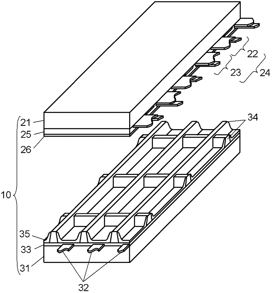
[0039] figure 1 It is an exploded perspective view showing the structure of the panel 10 in Embodiment 1 of this invention. On front panel 21 made of glass, a plurality of display electrode pairs 24 including scan electrodes 22 and sustain electrodes 23 are formed. Furthermore, dielectric layer 25 is formed to cover scan electrodes 22 and sustain electrodes 23 , and protective layer 26 is formed on dielectric layer 25 .
[0040] In addition, in order to reduce the discharge start voltage in the discharge cell, the protective layer 26 is formed of a material mainly composed of MgO, which is effective as a panel material. In this case, the secondary electron emission coefficient is large and the durability is excellent.
[0041] A plurality of data electrodes 32 are formed on rear plate 31 , dielectric layer 33 is formed to cover data electrodes 32 , and grid-shaped partition walls 34 are further formed thereon. Phosphor layers 35 that emit light of each color of red (R), gre...
Embodiment approach 2
[0134] The luminance in each subfield can be represented by the following equation. Hereinafter, the brightness generated by one discharge is referred to as "emission brightness", and the brightness obtained by repeated discharge is referred to as "brightness". (brightness of subfield)=(brightness based on sustain discharge generated in the sustain period of the subfield)+(light emission luminance based on address discharge generated in the address period of the subfield)
[0135] The discharge intensity of the address discharge varies with the number of address operations. This is because the wall charges decrease more as the elapsed time from the initializing operation to the writing operation becomes longer. Therefore, since the amount of decrease in wall charge is small for discharge cells that are performed earlier in the address operation, the discharge intensity of the address discharge is stronger, and the luminance of light emitted by the address discharge is also re...
PUM
 Abstract
Description
Claims
Application Information


