Grid driving unit circuit, grid driving circuit of grid driving unit circuit, and display

A unit circuit and gate drive technology, applied in the electronic field, can solve the problems of increasing the TFT voltage bias time in the gate drive circuit, shortening the service life of the gate drive circuit, etc., and achieve the effect of small number of components and simple structure

Active Publication Date: 2012-12-19
PEKING UNIV SHENZHEN GRADUATE SCHOOL +1
View PDF5 Cites 42 Cited by
  • Summary
  • Abstract
  • Description
  • Claims
  • Application Information

AI Technical Summary

Problems solved by technology

The second method above can reduce the number of TFTs, but the number of control signals increases, and these newly added control signals will increase the voltage bias time of TFTs in the gate drive circuit, shortening the service life of the gate drive circuit

Method used


Image

  • Grid driving unit circuit, grid driving circuit of grid driving unit circuit, and display
  • Grid driving unit circuit, grid driving circuit of grid driving unit circuit, and display
  • Grid driving unit circuit, grid driving circuit of grid driving unit circuit, and display

Examples


Embodiment 1

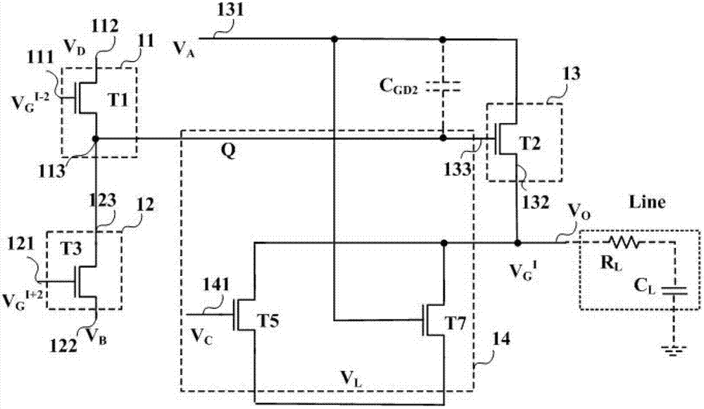
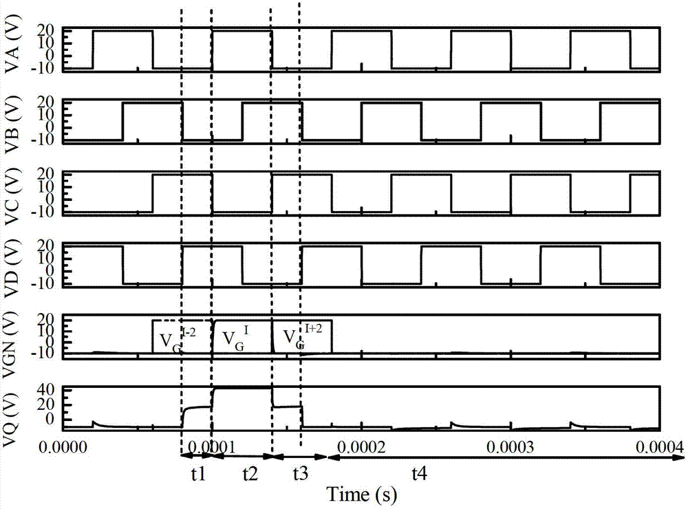
[0045] Please refer to figure 1 , the gate drive unit circuit in this embodiment includes: a gate scanning signal output terminal V O , a first module 11 , a second module 12 , a driving module 13 and a low level maintaining module 14 .

[0046] Gate scan signal output terminal V O Used to output the gate scan signal V G I , each gate driving unit circuit is coupled to a corresponding gate line, and the gate scanning signal output by the gate driving unit is applied to the gate line.

[0047] The first module 11 includes a fifth control signal input terminal 111 for inputting a fifth control signal, a fourth control signal input terminal 112 for inputting a fourth control signal, and an output terminal 113, the output terminal 113 of which is connected to the control node Q . The fourth control signal and the fifth control signal have a high-level overlap period within one frame, and the first module 11 responds to the high-level overlap of the fourth control signal and t...

Embodiment 2

[0081] Please refer to Figure 4 , is a circuit diagram of the gate driving unit circuit of this embodiment.

[0082] The difference between this embodiment and Embodiment 1 is that the low level maintaining module 14 of the gate drive unit circuit further includes: a fourth transistor T4, a sixth transistor T6, a first capacitor C1 and a second capacitor C2, the first Capacitor C1 is connected between control node Q and gate scan signal output terminal V O Between, the second capacitor C2 is connected between the gate of the seventh transistor T7 and the first control signal input terminal 131; the gate of the fourth transistor T4 is coupled to the first control signal input terminal 131 for inputting the first clock Signal V A , the first terminal is coupled to the control node Q, and the second terminal is coupled to the gate scanning signal output terminal V O ; The gate of the sixth transistor T6 is coupled to the gate scanning signal output terminal V O , the first e...

Embodiment 3

[0088] Please refer to Figure 5 , this embodiment provides a gate drive circuit, including N cascaded gate drive unit circuits as described in Embodiment 1 or Embodiment 2, where N is an integer greater than 1. The gate driving unit circuits are arranged on two sides A-A and B-B of the display panel (eg AM TFT panel).

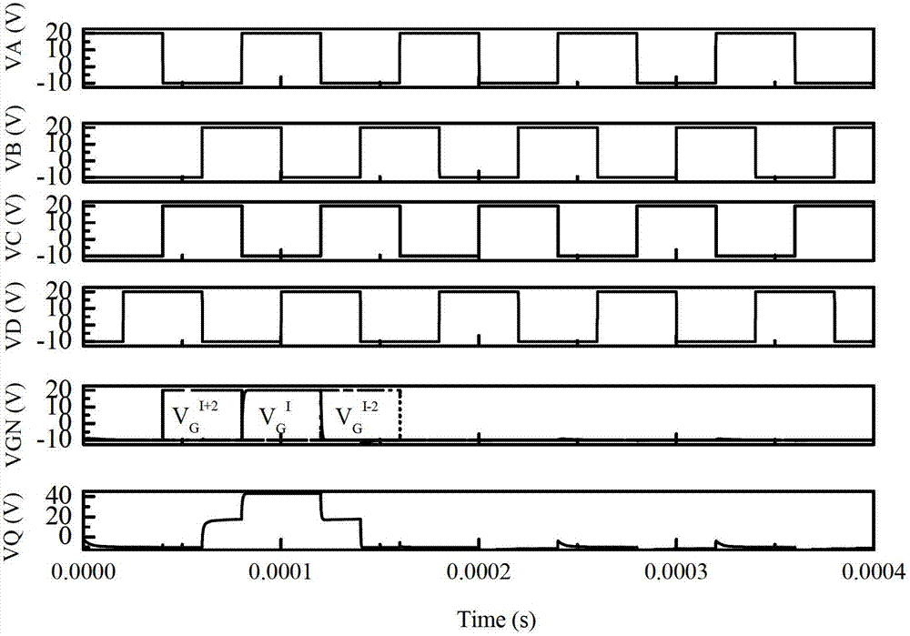
[0089] Four clock signal lines (CLK1, CLK2, CLK3, CLK4), in forward scanning mode, the first clock signal line CLK1, the second clock signal line CLK2, the third clock signal line CLK3 and the fourth clock signal line CLK4 The clocks are sequentially late by one phase; in the reverse scanning mode, the clocks of the first clock signal line CLK1 , the second clock signal line CLK2 , the third clock signal line CLK3 and the fourth clock signal line CLK4 are sequentially early by one phase. The first control signal input terminal V of the first stage gate driving unit circuit 401 A , the second control signal input terminal V B , the third control signal input...


PUM


Abstract

The invention discloses a grid driving unit circuit, a grid driving circuit of the grid driving unit circuit, and a display. The grid driving unit circuit comprises a grid scanning signal output end, a first module, a second module, a driving module and a low level maintaining module. By designing control signals, the first module is used for electricity charging in a forward scanning mode and electricity discharging in a reverse scanning mode; the second module is used for the electricity charging in the forward scanning mode and the electricity discharging in the reverse scanning mode; and the grid driving circuit is enabled to realize the forward or reserve scanning by adopting only one set of circuit through the multiplexing of the first module, the second module, the driving module and the low level maintaining module; and the number of used devices is small, and the structure is simple.

Description

technical field [0001] The present application relates to the field of electronics, in particular to a display and its gate drive circuit and gate drive unit circuit. Background technique [0002] Thin Film Transistor (Thin Film Transistor, TFT) flat panel display (Flat Panel Display, FPD) is the mainstream of display technology today. Integrated gate drive circuit is a new technology emerging in the vigorous development of TFT FPD industry. The advantages of this new technology of integrating the gate drive circuit on the display substrate (such as glass) include: reducing the number of peripheral drive chips and their pressing and sealing processes, which is conducive to the realization of narrower borders of the panel and improved The aesthetics of the display; the display module is simplified, the mechanical and electrical reliability of the display is enhanced; and it is possible to simplify the source drive circuit, improve the resolution of the display panel, and inc...

Claims


Application Information

Patent Timeline
Patent Type & Authority Applications(China)
IPC IPC(8): G09G3/36G09G3/32G09G3/3208
Inventor 张盛东廖聪维郑灿戴文君钟德镇简庭宪
Owner PEKING UNIV SHENZHEN GRADUATE SCHOOL
Why Eureka
Try Eureka