Silicon carbide semiconductor device and method for manufacturing same

A silicon carbide and semiconductor technology, applied in the field of silicon carbide semiconductor devices, can solve problems such as increased on-resistance and narrowed current path

Active Publication Date: 2012-12-26
DENSO CORP +1
View PDF6 Cites 16 Cited by
  • Summary
  • Abstract
  • Description
  • Claims
  • Application Information

AI Technical Summary

Problems solved by technology

[0006] Although the structure equipped with a p-type deep layer as described in Patent Document 1 is effective for preventing electric field concentration to the gate insulating film, the p-type deep layer narrows the current path and forms between two p-type deep layers adjacent to each other JFET area, resulting in increased on-resistance

Method used


Image

  • Silicon carbide semiconductor device and method for manufacturing same
  • Silicon carbide semiconductor device and method for manufacturing same
  • Silicon carbide semiconductor device and method for manufacturing same

Examples


no. 1 example )

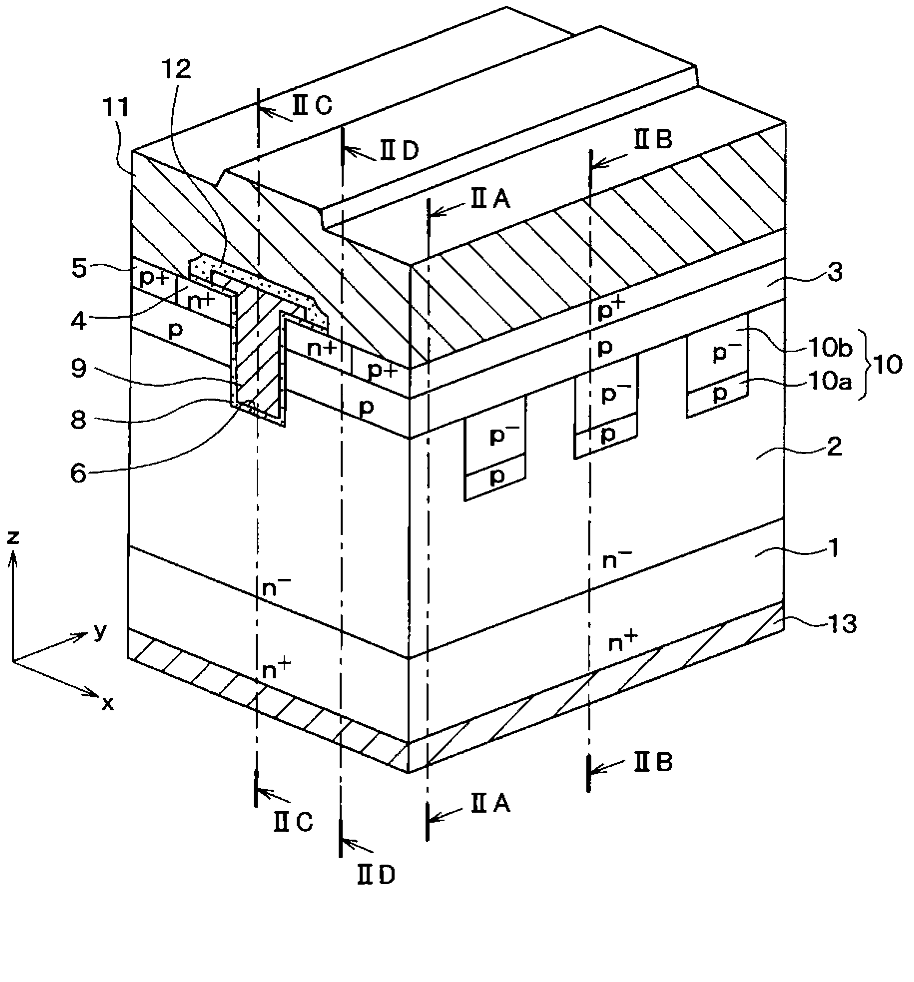
[0094] Next, the first embodiment will be described. Here, a MOSFET having an inverted trench gate structure will be introduced as an element equipped with a SiC semiconductor device.

[0095] figure 1 is a perspective cross-sectional view of a MOSFET having a trench gate structure according to the present embodiment. This figure corresponds to one unit of MOSFET. Although only one cell of the MOSFET is shown in this figure, it has the same figure 1 The structure of the MOSFET is similar to that of two or more columns of MOSFETs that are arranged adjacent to each other. Figures 2A to 2D yes figure 1 Cross-sectional view of the MOSFET. Figure 2A With figure 1 The xz plane in is taken parallel along the line IIA-IIA figure 1 section view of Figure 2B With figure 1 The xz plane in is parallel to the cross-sectional view taken along the line IIB-IIB; Figure 2C With figure 1 in the yz plane parallel to the intercept along the line IIC-IIC figure 1 sectional view of;...

no. 2 example )

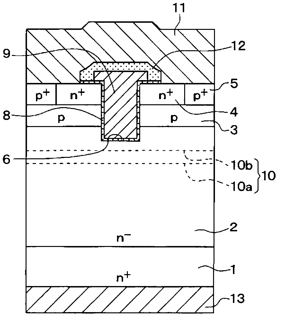
[0132] Next, the second embodiment will be described. The SiC semiconductor device of the present embodiment differs from the first embodiment in the structure of the p-type deep layer 10 . Since they are similar in basic structure, only the parts different from the first embodiment will be described next.

[0133] Image 6 is a perspective sectional view of the SiC semiconductor device according to the present embodiment. Figure 7A With Image 6 The xz plane in is parallel to the profile taken along the line VIIA-VIIA, while Figure 7B With Image 6 The cross-sectional view taken along the line VIIB-VIIB parallel to the yz plane in .

[0134] In this example, if Image 6 as well as Figure 7A with 7B As shown, the depth of the lightly doped region 10b of the p-type deep layer 10 is made shallower than that in the first embodiment, and the bottom of the trench 6 is in contact with the heavily doped region 10a. In this structure, when a voltage is applied to the gate ...

no. 3 example )

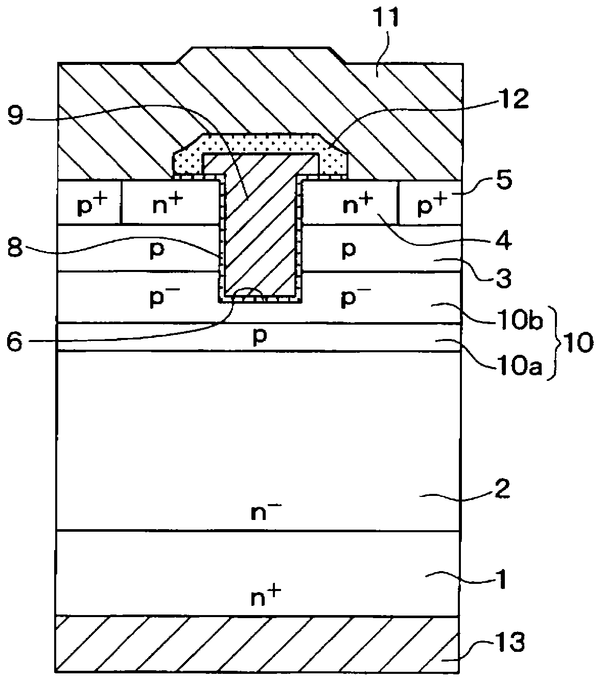
[0137] Next, a third embodiment will be described. The SiC semiconductor device of this embodiment is also different from the first embodiment in the structure of the p-type deep layer 10 . Since they are similar in basic structure, only the parts different from the first embodiment will be described next.

[0138] Figure 8 is a perspective sectional view of the SiC semiconductor device according to the present embodiment. Figure 9A With Figure 8 The xz plane in is parallel to the profile taken along the line IXA-IXA, while Figure 9B With Figure 8 The cross-sectional view taken along the line IXB-IXB parallel to the yz plane in .

[0139] In this example, if Figure 8 as well as Figure 9A with 9B As shown, the lower and upper layers of the p-type deep layer 10 are formed as a lightly doped region 10b, and the middle layer is formed as a heavily doped region 10a. In this structure, when a voltage is applied to the gate electrode 9, inversion occurs only in the li...


PUM


Abstract

A SiC device includes an inversion type MOSFET having: a substrate, a drift layer, and a base region stacked in this order; source and contact regions in upper portions of the base region; a trench penetrating the source and base regions; a gate electrode on a gate insulating film in the trench; a source electrode coupled with the source and base region; a drain electrode on a back of the substrate; and multiple deep layers in an upper portion of the drift layer deeper than the trench. Each deep layer has an impurity concentration distribution in a depth direction, and an inversion layer is provided in a portion of the deep layer on the side of the trench under application of the gate voltage.

Description

[0001] Cross References to Related Applications [0002] This application is based on Japanese Patent Application No. 2011-27997 filed on February 11, 2011, the disclosure of which is incorporated herein by reference. technical field [0003] The present disclosure relates to a silicon carbide semiconductor device having a trench gate type MOSFET, and a method for manufacturing a silicon carbide semiconductor device having a trench gate type MOSFET. Background technique [0004] In SiC semiconductor devices, increasing channel density is effective for supplying larger currents. Therefore, a MOSFET having a trench gate structure has been adopted and put into practical use as a silicon transistor. It goes without saying that this trench gate structure can be applied to SiC semiconductor devices. However, serious problems occur when it is applied to SiC. Specifically, SiC has a breakdown field strength ten times that of silicon, and thus a SiC semiconductor device is used wh...

Claims


Application Information

Patent Timeline
Patent Type & Authority Applications(China)
IPC IPC(8): H01L29/10H01L29/78H01L29/739H01L29/16H01L21/336H01L29/66
CPCH01L29/66068H01L29/0878H01L29/7397H01L29/0634H01L29/1095H01L29/1608H01L29/66348H01L29/7813
Inventor 登尾正人山本建策松木英夫高谷秀史杉本雅裕副岛成雅石川刚渡边行彦
Owner DENSO CORP
Why Eureka
Try Eureka