Silicon carbide semiconductor device and method for manufacturing the same

Inactive Publication Date: 2012-12-20
DENSO CORP +1
View PDF3 Cites 27 Cited by
  • Summary
  • Abstract
  • Description
  • Claims
  • Application Information

AI Technical Summary

Benefits of technology

[0013]In the above method, since the current flowing through the channel flows not only the channel but also the inversion layer formed in th

Problems solved by technology

A serious problem however occurs when it is applied to SiC.
As a result, an electric field ten times that of the silicon device is a

Method used


Image

  • Silicon carbide semiconductor device and method for manufacturing the same
  • Silicon carbide semiconductor device and method for manufacturing the same
  • Silicon carbide semiconductor device and method for manufacturing the same

Examples


Example

[0090]A first embodiment will next be described. Here, a MOSFET with an inversion type trench gate structure will be described as an element which a SiC semiconductor device is equipped with.

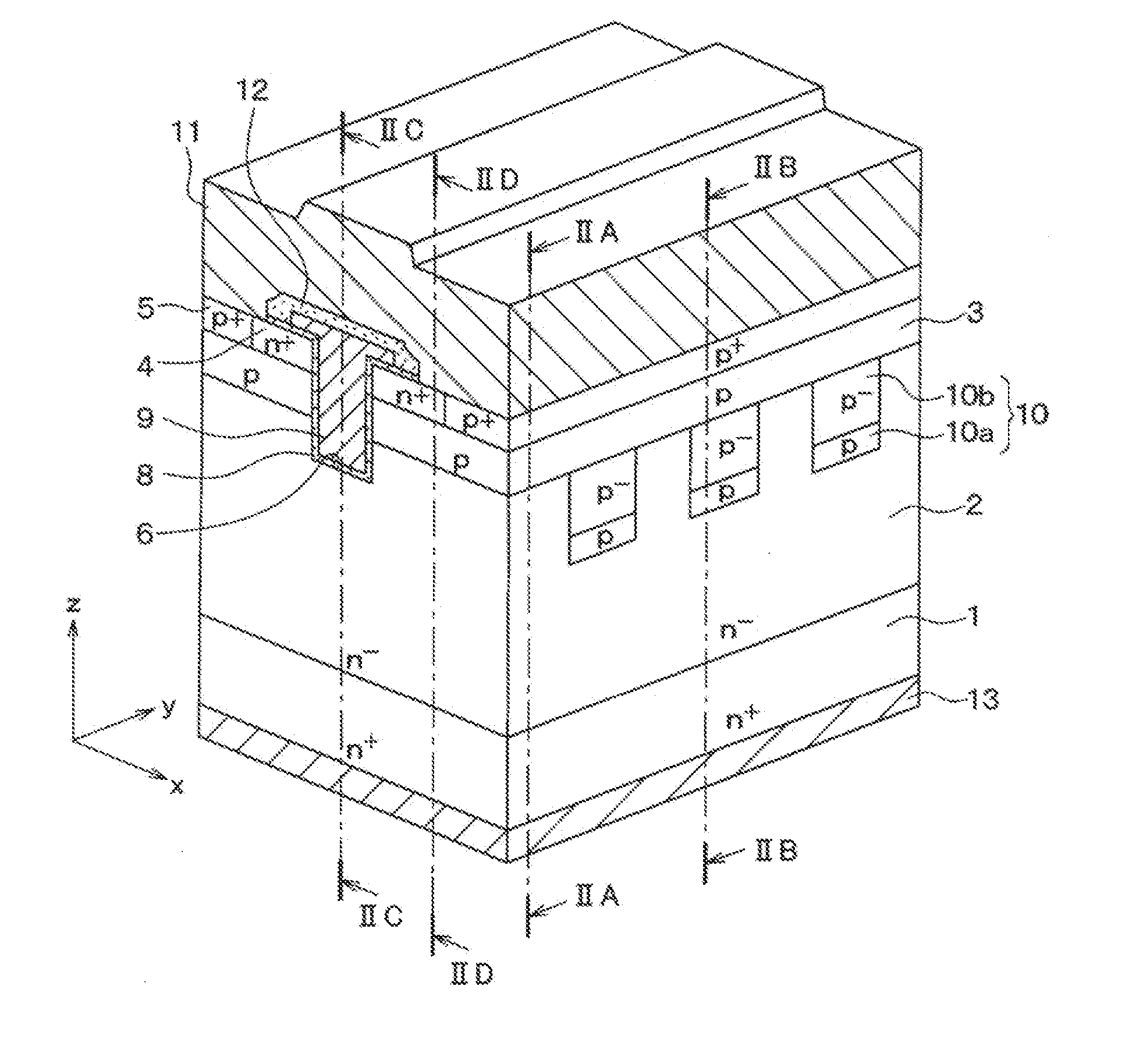
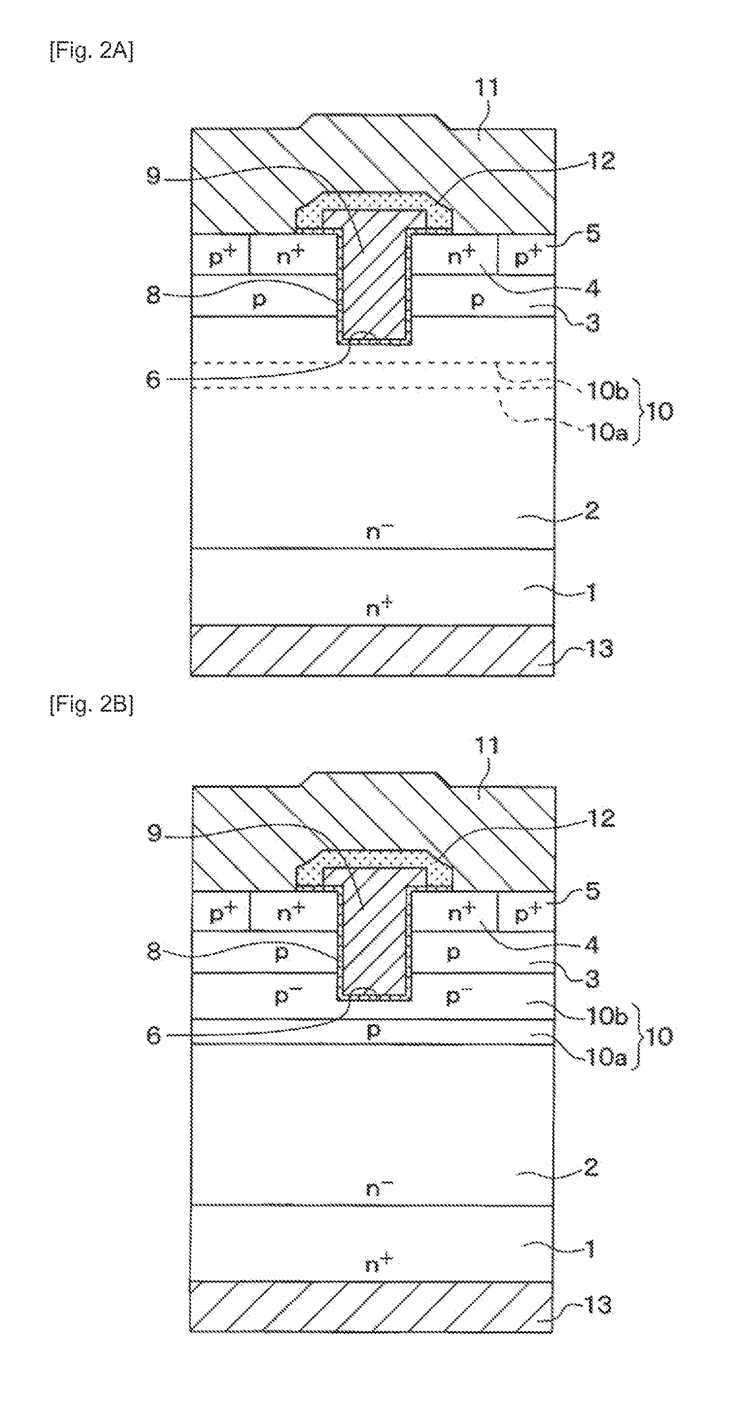
[0091]FIG. 1 is a perspective cross-sectional view of a MOSFET having a trench gate structure according to the present embodiment. This drawing corresponds to one cell of the MOSFET. Although only one cell of the MOSFET is shown in this diagram, two or more columns of MOSFETs having a similar structure to that of the MOSFET of FIG. 1 are arranged adjacent to each other. FIGS. 2A to 2D are cross-sectional views of the MOSFET of FIG. 1. FIG. 2A is a cross-sectional view of FIG. 1 taken along the line IIA-IIA in parallel with the xz plane in FIG. 1; FIG. 2B is a cross-sectional view taken along the line IIB-IIB in parallel with the xz, plane in FIG. 1, FIG. 2C is a cross-sectional view of FIG. 1 taken along the line IIC-IIC in parallel with the yz plane in FIG. 1, and FIG. 2D is a cross-sectional v...

Example

Second Embodiment

[0127]A second embodiment will next be described. The SiC semiconductor device of this embodiment is different from that of the first embodiment in the structure of the p type deep layer 10. Since they are similar in the fundamental structure, only portions different from the first embodiment will next be described.

[0128]FIG. 6 is a perspective cross-sectional view of the SiC semiconductor device according to this embodiment. FIG. 7A is a cross-sectional view taken along the line VIIA-VIIA in parallel with the xz plane in FIG. 6 and FIG. 713 is a cross-sectional view taken along the line VIIB-VIIB in parallel with the yz plane in FIG. 6.

[0129]In this embodiment, as shown in FIG. 6 and FIGS. 7A and 713, the depth of the lightly doped region 10b of the p type deep layer 10 is made shallower than that in the first embodiment and the bottom of the trench 6 is in contact with the heavily doped region 10a. In such a structure, when a voltage is applied to the gate electr...

Example

[0131]A third embodiment will next he described. The SiC semiconductor device of this embodiment is also different from that of the first embodiment in the structure of the p type deep layer 10. Since they are similar in the fundamental structure, only portions different from the first embodiment will next be described.

[0132]FIG. 8 is a perspective cross-sectional view of the SiC semiconductor device according to the present embodiment. FIG. 9A is a cross-sectional view taken along the line IXA-IXA in parallel with the xz plane in FIG. 8 and FIG. 9B is a cross-sectional view taken along the line IXB-IXB in parallel with the yz plane in FIG. 8.

[0133]In this embodiment, as shown in FIG. 8 and FIGS. 9A and 9B, the lower layer portion and the upper layer portion of the p type deep layer 10 are formed as a lightly doped region 10b, while the intermediate layer portion is formed as the heavily doped region 10a. In such a structure, when a gate voltage is applied to the gate electrode 9, i...


PUM


Abstract

A SiC device includes an inversion type MOSFET having: a substrate, a drift layer, and a base region stacked in this order; source and contact regions in upper portions of the base region; a trench penetrating the source and base regions; a gate electrode on a gate insulating film in the trench; a source electrode coupled with the source and base region; a drain electrode on a back of the substrate; and multiple deep layers in an upper portion of the drift layer deeper than the trench. Each deep layer has an impurity concentration distribution in a depth direction, and an inversion layer is provided in a portion of the deep layer on the side of the trench under application of the gate voltage.

Description

CROSS REFERENCE TO RELATED APPLICATION [0001]This application is based on Japanese Patent Application No. 2011-27997 filed on Feb. 11, 2011, the disclosure of which is incorporated herein by reference.TECHNICAL FIELD [0002]The present disclosure relates to a silicon carbide semiconductor device having a trench gate type MOSFET and a method for manufacturing a silicon carbide semi-conductor device having a trench gate type MOSFET,BACKGROUND ART [0003]SiC semiconductor devices, an increase in channel density is effective for providing a greater electric current. A MOSFET with a trench gate structure has therefore been adopted and already been put to practical use in silicon transistors. Needless to say, this trench gate structure can be applied to a SiC semiconductor device. A serious problem however occurs when it is applied to SiC. Described specifically, SiC has breakdown field strength ten times that of silicon so that a SiC semiconductor device is used while applying a voltage ab...

Claims


Application Information

Patent Timeline
IPC IPC(8): H01L29/24H01L21/336
CPCH01L29/0634H01L29/0878H01L29/1095H01L29/7813H01L29/66068H01L29/66348H01L29/7397H01L29/1608
Inventor NOBORIO, MASATOYAMAMOTO, KENSAKUMATSUKI, HIDEOTAKAYA, HIDEFUMISUGIMOTO, MASAHIROSOEJIMA, NARUMASAISHIKAWA, TSUYOSHIWATANABE, YUKIHIKO
Owner DENSO CORP
Why Eureka
Try Eureka