Silicon carbide MOS device with groove type JFET and preparation process thereof

A MOS device and preparation technology, which is applied in semiconductor/solid-state device manufacturing, semiconductor devices, electrical components, etc., can solve the problems of increasing the proportion of on-resistance in the JFET area of ​​the device, poor short-circuit characteristics of the device, and reducing the size of the cell. Achieve the effects of reducing the number of photolithography, low JFET resistance, and reducing channel resistance

Pending Publication Date: 2020-08-07
PN JUNCTION SEMICON HANGZHOU CO LTD
View PDF0 Cites 2 Cited by
  • Summary
  • Abstract
  • Description
  • Claims
  • Application Information

AI Technical Summary

Problems solved by technology

However, while reducing the size of the cell, it is also increasing the proportion of on-resistance in the JFET area of ​​the device.
At the same time, the higher channel density also makes the device have a higher saturation current, resulting in poor short-circuit characteristics of the device

Method used


Image

  • Silicon carbide MOS device with groove type JFET and preparation process thereof
  • Silicon carbide MOS device with groove type JFET and preparation process thereof
  • Silicon carbide MOS device with groove type JFET and preparation process thereof

Examples


Embodiment Construction

[0042] The following will clearly and completely describe the technical solutions in the embodiments of the present invention with reference to the accompanying drawings in the embodiments of the present invention. Obviously, the described embodiments are some of the embodiments of the present invention, but not all of them. Based on the embodiments of the present invention, all other embodiments obtained by persons of ordinary skill in the art without making creative efforts belong to the protection scope of the present invention.

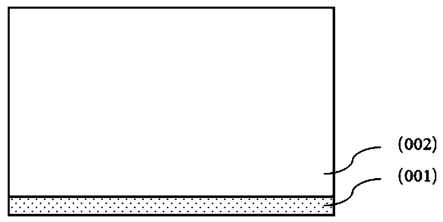
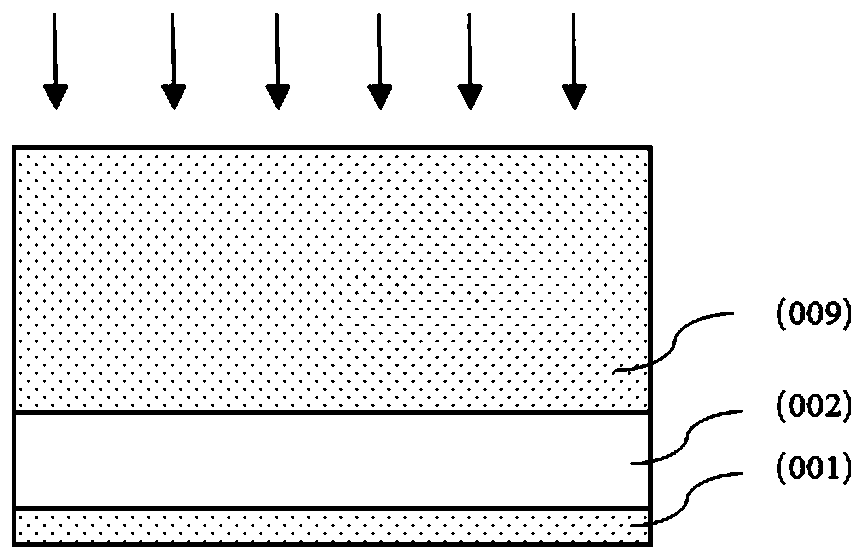
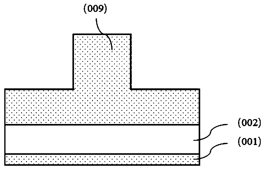
[0043] The embodiment of the present invention discloses a flow chart of the preparation process of a silicon carbide MOS device with a grooved JFET, including the following steps:

[0044] (a) see figure 1 and figure 2 , a first conductivity type semiconductor epitaxial layer 002 is provided on the front surface of the silicon carbide substrate 001, wherein the doping type of the material of the silicon carbide substrate 001 is the first conduc...


PUM


Abstract

The invention discloses a silicon carbide MOS device with a groove type JFET and a preparation process of the silicon carbide MOS device. The silicon carbide MOS device with the groove type JFET comprises a silicon carbide substrate, the doping type of the silicon carbide substrate material is a first conductive type, a first conductive type semiconductor epitaxial layer and a drain electrode arerespectively arranged on a front surface and a back surface of the silicon carbide substrate, wherein a JFET region is arranged on an active region of the first conductive type semiconductor epitaxiallayer, a first surface, a second surface and a third surface are arranged on the JFET region, and a first conductive type source region and a second conductive type base region are arranged on the first surface and the second surface respectively from outside to inside, a source electrode is arranged above the first surface, a gate medium and a gate electrode are arranged above the third surface,a second conductive type injection body region is arranged between the second conductive type base region and the source electrode, and an inter-electrode isolation medium is arranged between the source electrode and the gate electrode.

Description

technical field [0001] The invention belongs to the technical field of semiconductors, and in particular relates to a silicon carbide MOS device with a slot-type JFET and a preparation process thereof. Background technique [0002] MOS field effect transistor power devices made of silicon carbide (SiC) can withstand higher voltages and faster switching speeds than Si devices. Since silicon carbide is often used in high-voltage applications, the doping concentration of its epitaxial layer is relatively low, which makes the JFET resistance in the MOSFET account for a large proportion of the total on-resistance, which increases the on-resistance and conduction loss of the MOS device. Not only that, due to the high manufacturing cost of SiC MOS and the difficulty of channel definition, how to obtain a narrower channel under the condition of reducing the number of photolithography has become a difficulty in the mass production of SiC MOS devices at this stage. [0003] Due to th...

Claims


Application Information

Patent Timeline
Patent Type & Authority Applications(China)
IPC IPC(8): H01L29/06H01L29/78H01L21/336
CPCH01L29/0684H01L29/66068H01L29/7827
Inventor 陈欣璐黄兴陈然
Owner PN JUNCTION SEMICON HANGZHOU CO LTD
Why Eureka
Try Eureka