High-light transmittance transparent display device

A transparent display and high light transmittance technology, applied in optics, nonlinear optics, static indicators, etc., can solve the problems of halving the writing time of transparent sub-pixel signal voltage, reducing the complexity of pixel structure, etc. Transmittance, solving the effect of halving the writing time

Active Publication Date: 2013-01-02
NANJING CEC PANDA LCD TECH
View PDF5 Cites 17 Cited by
  • Summary
  • Abstract
  • Description
  • Claims
  • Application Information

AI Technical Summary

Problems solved by technology

[0004] Purpose of the invention: The purpose of the invention is to solve the problem of halving the writing time of the transparent sub-pixel signal voltage and reduce the complexity of the pixel structure and the complexity of the driving system

Method used


Image

  • High-light transmittance transparent display device
  • High-light transmittance transparent display device
  • High-light transmittance transparent display device

Examples


Embodiment Construction

[0035] Below in conjunction with accompanying drawing and specific embodiment, further illustrate the present invention, should be understood that these embodiments are only for illustrating the present invention and are not intended to limit the scope of the present invention, after having read the present invention, those skilled in the art will understand various aspects of the present invention Modifications in equivalent forms all fall within the scope defined by the appended claims of this application.

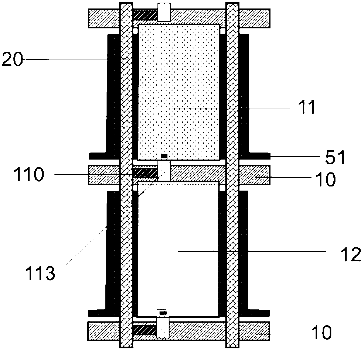
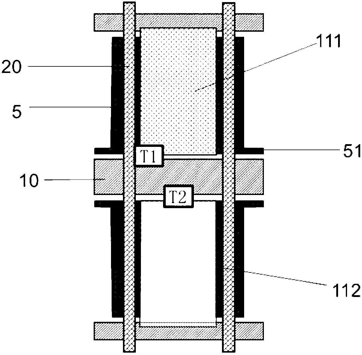
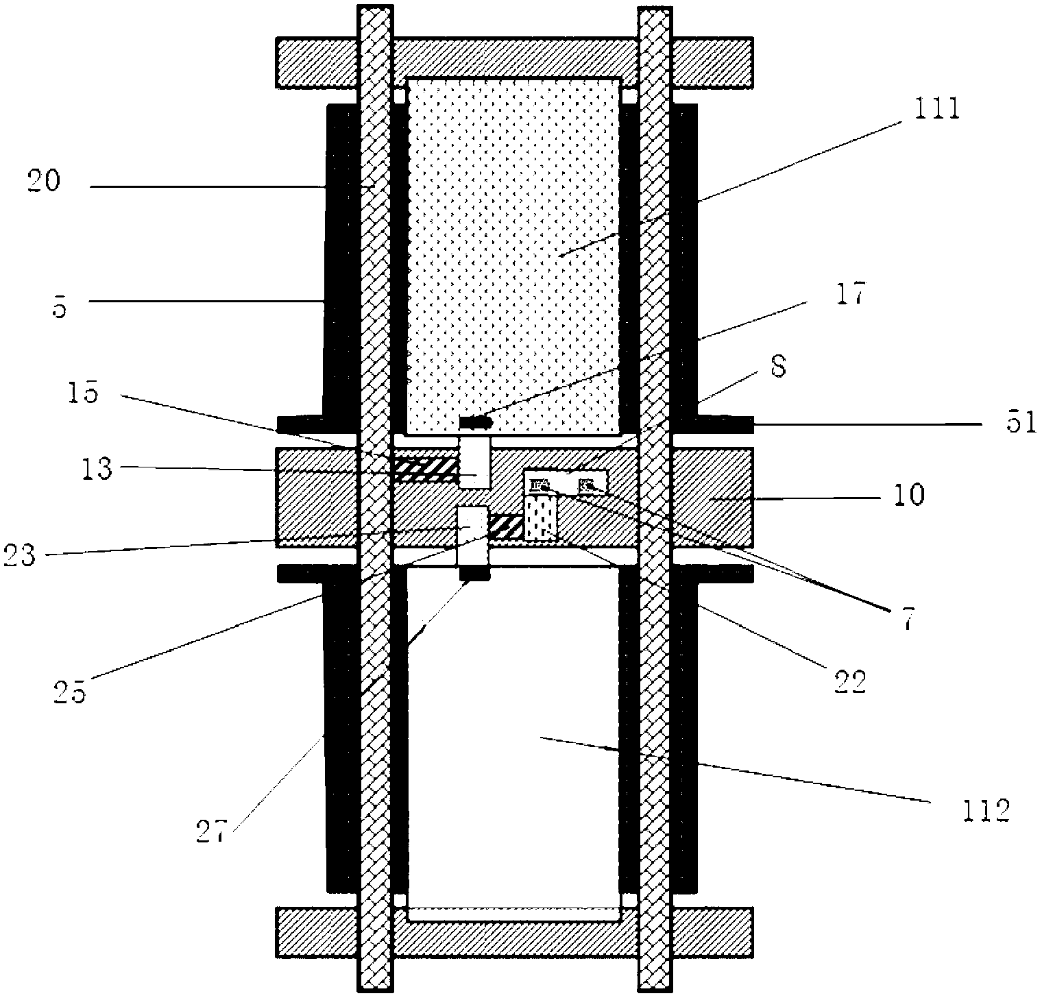
[0036] The invention relates to a display device with high light transmittance, comprising an active matrix substrate, a pair of opposing substrates opposite to the active matrix substrate, and a liquid crystal layer sandwiched between the two substrates, the active matrix substrate includes : several scanning lines; several data lines crossing the scanning lines; several common electrode lines parallel to the scanning lines; and several pixel units defined by the interse...


PUM


Abstract

The invention relates to a display device with high light transmittance. The display device comprises an active matrix substrate, an opposite substrate arranged opposite to the active matrix substrate, and a liquid crystal layer clamped between two substrates, wherein the active matrix substrate comprises a plurality of sub-pixel units; each sub-pixel unit comprises a first third-pixel unit for displaying color, a second third-pixel unit without color resistance, a first control element for controlling the first third-pixel unit, and a second control element for controlling the second third-pixel unit. According to the display device, the first third-pixel unit and the second third-pixel unit share one scanning line; with the adoption of the structure, the pixel structure and the complexity of a driving system are effectively reduced,; once the first control element and the second control element are driven, the first third-pixel unit displays the color of the input model; and the second third-pixel unit displays the lighter white state, therefore, the light transmittance of the transparent display device can be effectively improved.

Description

technical field [0001] The invention relates to a transparent display device with high light transmittance, in particular to a transparent display device with a pixel structure for transparent display. Background technique [0002] Transparent display is a new generation of panel technology, which enables the panel to have high light transmittance and combines physical information with virtual information. At present, transparent displays using LCD panels mainly use technologies such as high-transmittance color filters, additional white sub-pixels, and field color sequential methods. Among them, the high transmittance color film technology is used, and the color saturation and contrast of the transparent display will decrease; the existing scheme of using the technology of adding white sub-pixels is to increase the number of scanning lines, and the other is to increase the number of data lines. quantity to be realized. After the number of sub-pixel scanning lines doubles, ...

Claims


Application Information

Patent Timeline
Patent Type & Authority Applications(China)
IPC IPC(8): G02F1/1362G02F1/1368G02F1/133
Inventor 马群刚
Owner NANJING CEC PANDA LCD TECH
Why Eureka
Try Eureka