Pitch-variable clamp for wafer replacing
A variable pitch and fixture technology, applied in sustainable manufacturing/processing, electrical components, climate sustainability, etc., can solve the problems of high labor intensity, low efficiency, uncontrollable fragmentation rate, etc.
- Summary
- Abstract
- Description
- Claims
- Application Information
AI Technical Summary
Problems solved by technology
Method used
Image
Examples
Embodiment 1
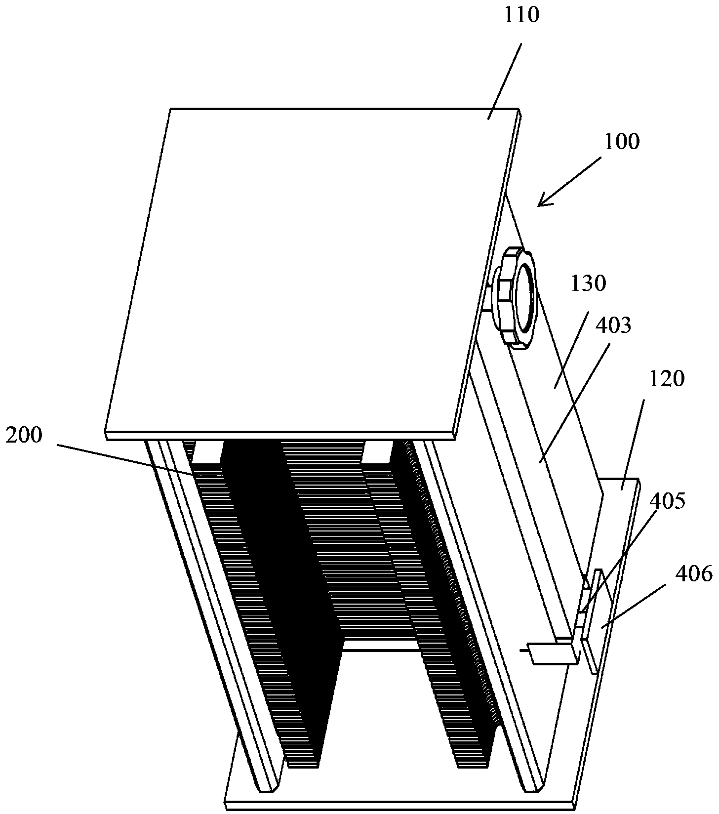
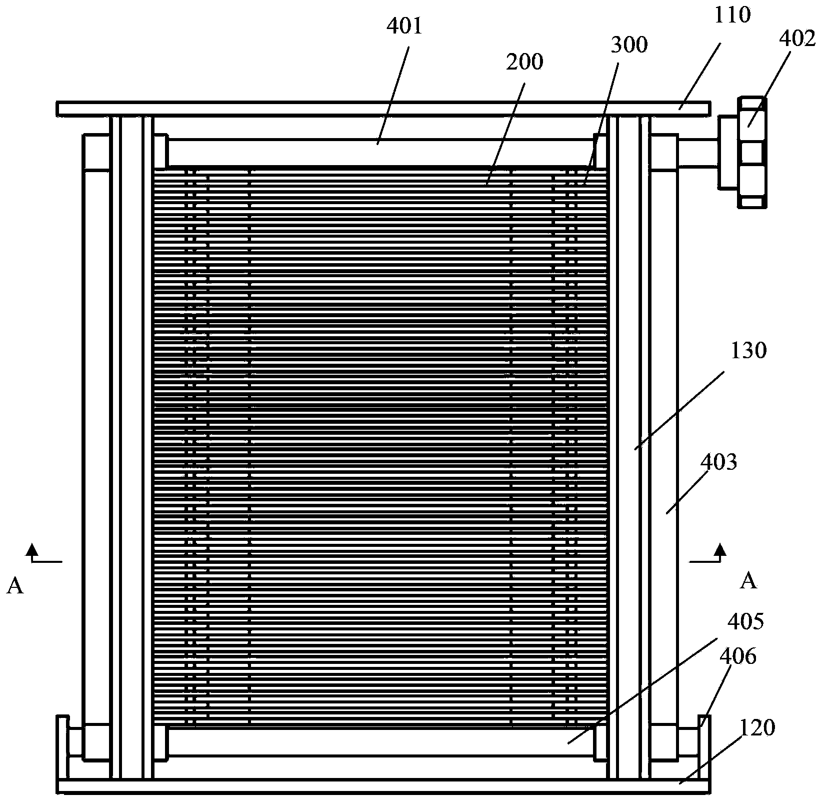
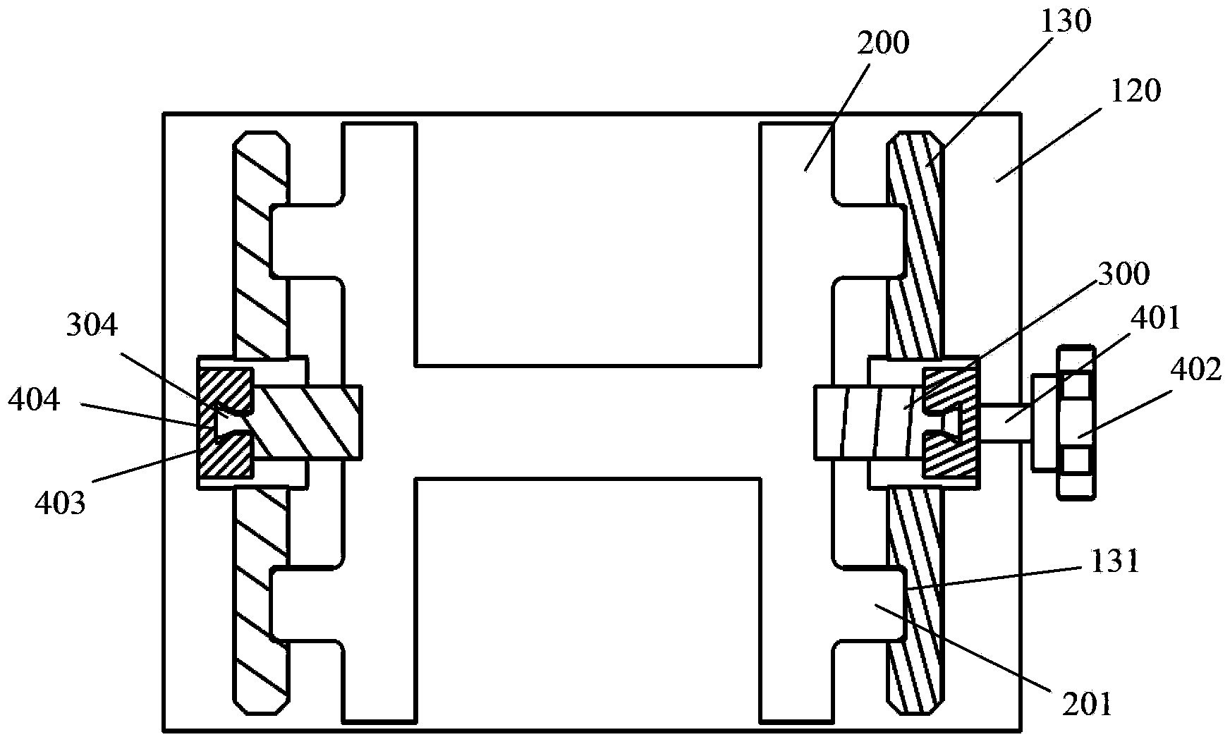
[0025] Such as figure 1 , figure 2 , image 3 As shown, the variable pitch jig for film rewinding of the present invention includes a frame 100, a multi-layer silicon wafer resting plate 200, spacers 300 and a driving mechanism.
[0026] The frame 100 is surrounded by a top plate 110 , a bottom plate 120 and two side plates 130 separated on the left and right sides. Openings are formed at the front and back of the frame 100 to allow silicon wafers to enter and exit.
[0027] Such as Figure 5 As shown, the inner surface of the side plate 130 has vertically extending slide grooves 131 on both sides, and has a vertically extending strip-shaped gap 132 in the middle.
[0028] Figure 6 As shown, the thickness of each silicon wafer resting plate 200 is 2 mm, and two protruding sliders 201 are respectively provided at both ends. to combine image 3 As shown, when the protruding slider 201 is assembled, it is located in the slide groove 131 of the side plate 130 . In this wa...
Embodiment 2
[0037] Such as Figure 10 , 11 , 12, the difference between this embodiment and embodiment 1 is that: the spacer 300 is circular and has a square hole 305 in the middle. The driving mechanism is two driving rods 501 with a square cross-section arranged on both sides of the silicon wafer resting plate, and each driving rod 501 passes through the clamping holes 305 of all spacers 300 on the same side in turn. A synchronous belt (not shown) is installed between the two driving rods 501 . Other structures are the same as in Embodiment 1. In this embodiment, the thick portion 302 of the spacer 300 is driven to be inserted into or pulled out of the gap between the silicon wafer resting racks by rotating the lever 501 . A timing belt is installed between the two driving rods 501 so that the driving rod 501 can drive the spacer 300 to rotate at the same time, ensuring that the thick part 302 of the spacer 300 on both sides can be inserted or pulled out between the silicon wafer res...
PUM
 Abstract
Description
Claims
Application Information


