Shift register circuit, display device, and method for driving shift register circuit
A technology for shift registers and display devices, applied in static memory, digital memory information, instruments, etc., can solve problems such as large over-excitation
- Summary
- Abstract
- Description
- Claims
- Application Information
AI Technical Summary
Problems solved by technology
Method used
Image

Examples
Embodiment 1
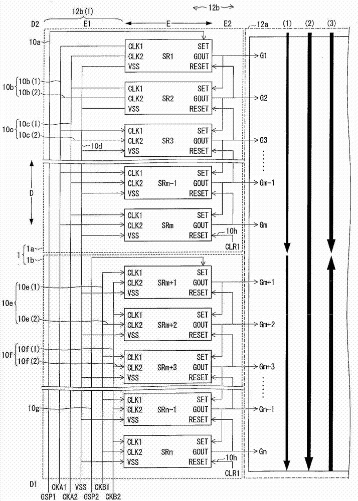
[0090] figure 1 The structure of the shift register circuit 1 of this embodiment is shown.
[0091] The shift register circuit 1 has a first circuit unit 1a, a second circuit unit 1b, and wirings 10a, 10b, 10c, 10d, 10e, 10f, 10g, and 10h.
[0092] The first circuit unit 1 a has a structure in which stages (shift register stages) SRk (k is a natural number of 1≦k≦m) are connected in cascade. Each stage SRk has a set terminal SET, an output terminal GOUT, a reset terminal RESET, a low power input terminal VSS, and clock input terminals CLK1, CLK2. In each stage of SRk (k≥2), the set terminal SET is input with the output signal Gk-1 of the preceding stage SRk-1. The gate start pulse signal GSP1 is input to the set terminal SET of the first stage SR1 of the first circuit portion 1a. In each stage SRk (1≤k≤m), the output terminal GOUT outputs an output signal Gk to the corresponding gate line GLk arranged in the active region 12a. In each stage SRk (k≦m−1), the reset terminal...
Embodiment 2
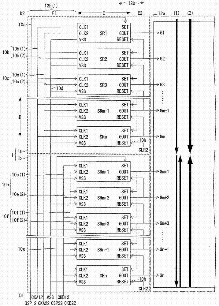
[0117] image 3 The structure of the shift register circuit 1 of this embodiment is shown.
[0118] image 3 The shift register circuit 1 is with figure 1 The shift register circuit has the same structure as 1, but instead of figure 1 Clock signals CKA1, CKA2, CKB1, CKB2, gate start pulse signals GSP1, GSP2, and clear signal CLR1 are input with clock signals (drive signals) CKA12, CKA22, CKB12, CKB22, and gate start Pulse signal GSP12, GSP22, clear signal CLR2.
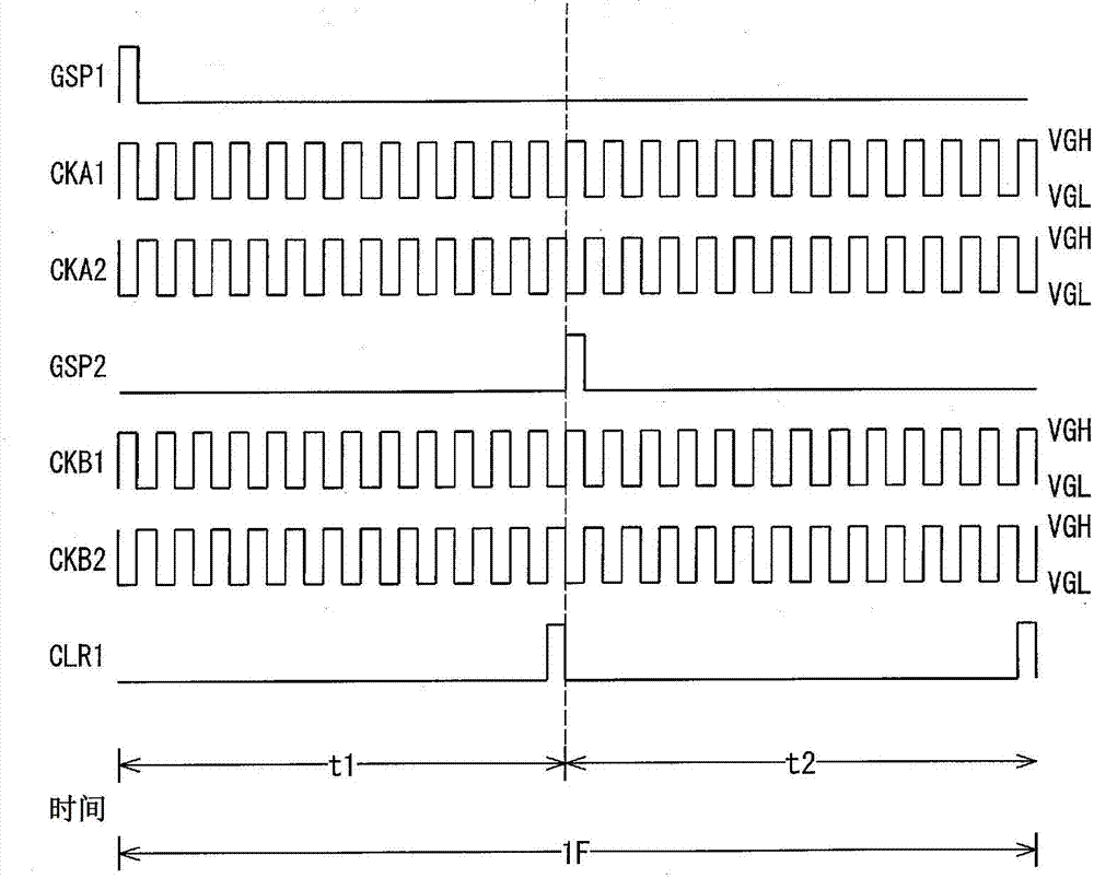
[0119] Figure 4 As shown, the duty ratio of the clock signals CKA12 , CKA22 , CKB12 , and CKB22 is the same as that of the clock signals CKA1 , CKA2 , CKB1 , and CKB2 , and their periods are doubled. The gate start pulse signals GSP1 and GSP2 are active during the first clock pulse period of one frame period (1F). The clear signal CLR2 becomes active during the last clock pulse period of one frame period (1F).
[0120] Thus, if image 3 As shown in (1), scanning can be performed simultaneously in the first ...
Embodiment 3
[0125] Figure 5 The structure of the shift register circuit 1 of this embodiment is shown.
[0126] Figure 5 The shift register circuit 1 is with figure 1 The shift register circuit has the same structure as 1, but instead of figure 1 Clock signals CKA1 , CKA2 , CKB1 , CKB2 , and clear signal CLR1 are input to clock signals (drive signals) CKA13 , CKA23 , CKB13 , CKB23 , and clear signal CLR3 in the order described.
[0127] Such as Figure 6 As shown, the clock signals CKA13 and CKA23 are signals in which the period t2 of the clock signals CKA1 and CKA2 is a rest period in which the inactive level is maintained. The clock signals CKB13 and CKB23 are signals in which the period t1 of the clock signals CKB1 and CKB2 is a rest period in which the inactive level is maintained. The clear signal CLR3 is a signal which becomes an active level only in the last clock pulse period of one frame period (1F).
[0128] Such as Figure 6 As shown in (1), the gate scanning is perf...
PUM
 Abstract
Description
Claims
Application Information
 - R&D Engineer
- R&D Manager
- IP Professional
- Industry Leading Data Capabilities
- Powerful AI technology
- Patent DNA Extraction
Browse by: Latest US Patents, China's latest patents, Technical Efficacy Thesaurus, Application Domain, Technology Topic.
© 2024 PatSnap. All rights reserved.Legal|Privacy policy|Modern Slavery Act Transparency Statement|Sitemap