On-line automatic detection device for silicon wafer
An automatic detection device and silicon wafer technology, applied in the direction of testing moving boards, sorting, etc., can solve the problems of easy debris, low detection efficiency, high labor costs, etc., and achieve the effect of low cost and high efficiency
- Summary
- Abstract
- Description
- Claims
- Application Information
AI Technical Summary
Problems solved by technology
Method used
Image

Examples
Embodiment Construction
[0020] Below in conjunction with the embodiment shown in the accompanying drawings, the present invention is described in detail as follows:
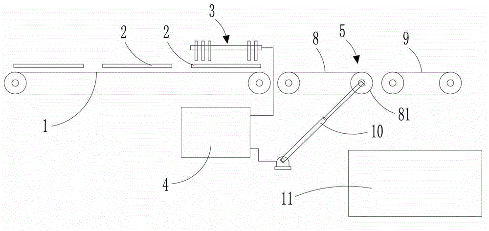
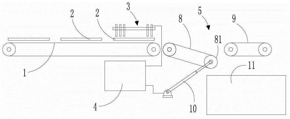
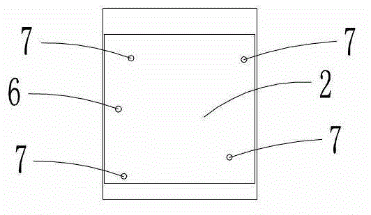
[0021] as attached figure 1 and attached figure 2 As shown, the silicon wafer online automatic detection device of the present invention is used to detect whether a number of silicon wafers 2 transmitted synchronously and sequentially with the transmission line 1 are fragments and sort the fragments from the transmission line 1. The structure includes a detection device arranged above the transmission line 1 Unit 3, the control unit 4 connected with the detection unit 3 signal and the sorting unit 5 connected with the control unit 4 signal, the detection unit 3 includes a first detection piece for detecting whether there is a silicon chip 2 on the transmission line 1 at present, for Detect that the corresponding current silicon wafer 2 is a second detection piece of a fragment or a complete piece; the sorting unit 5 includes a s...
PUM
 Abstract
Description
Claims
Application Information
 - R&D Engineer
- R&D Manager
- IP Professional
- Industry Leading Data Capabilities
- Powerful AI technology
- Patent DNA Extraction
Browse by: Latest US Patents, China's latest patents, Technical Efficacy Thesaurus, Application Domain, Technology Topic.
© 2024 PatSnap. All rights reserved.Legal|Privacy policy|Modern Slavery Act Transparency Statement|Sitemap