Non-film jig and application of non-film process in manufacturing process of chip on board (COP)

A fixture and process technology, applied in semiconductor/solid-state device manufacturing, electrical components, circuits, etc., can solve problems such as adhesion and inability to be removed, reduce the proportion of black spots, improve cleaning yield, and improve cleaning yield Effect

Active Publication Date: 2015-04-08
NINGBO SUNNY OPOTECH CO LTD
View PDF4 Cites 0 Cited by
  • Summary
  • Abstract
  • Description
  • Claims
  • Application Information

AI Technical Summary

Problems solved by technology

[0003] The invention provides an application of a filmless process in the COB manufacturing process, which overcomes the problem that sticky particles of the adhesive tape adhere to the surface of the chip and cannot be removed during the cleaning process. The technical solution is as follows:

Method used


Image

  • Non-film jig and application of non-film process in manufacturing process of chip on board (COP)
  • Non-film jig and application of non-film process in manufacturing process of chip on board (COP)
  • Non-film jig and application of non-film process in manufacturing process of chip on board (COP)

Examples


Embodiment Construction

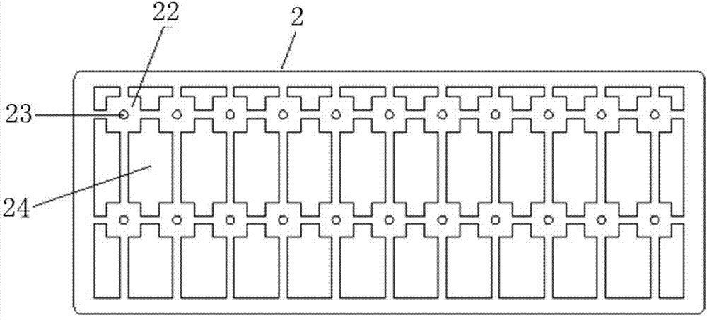
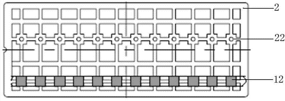
[0017] figure 1 It is a schematic diagram of the filmless metallurgical tool in the embodiment of the present invention, such as figure 1 As shown, the filmless fixtures used in the cleaning and cleaned in the COB process include a frame 2, a bearing surface 22, and a hollowed out part 24. The bearing surface 22 is evenly arranged in the frame, and its center position is provided with a A hollow portion 24 is formed between the glue hole 23 and the bearing surface 22 .

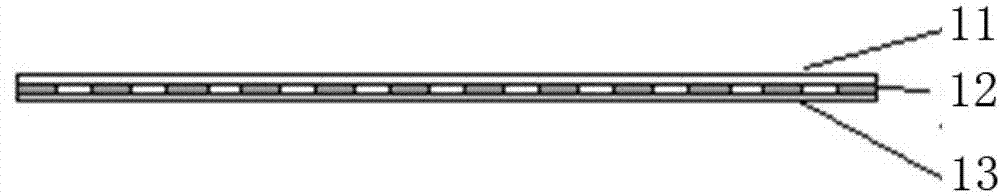
[0018] figure 2 It is a schematic diagram of the double-sided adhesive tape in the embodiment of the present invention. The double-sided adhesive tape used for cleaning in the COB process includes a first release film 11, an adhesive tape 12, and a second release film 13. The adhesive tape 12 is arranged in sections. The adhesive force between the first release film 11 and the adhesive tape 12 is smaller than that of the second release film 13 .

[0019] Wherein, the adhesive tape 13 corresponds to the car...


PUM


Abstract

The invention provides application of non-film process in the manufacturing process of chip on board (COP), which comprises the following steps: 1) tearing down a release film on one side of a double-sided adhesive tape and adhering the release film to a non-film jig, wherein the bearing surface of the non-film jig is correspondingly adhered to the double-sided adhesive tape; the double-sided adhesive tape comprises a first release film, an adhesive tape and a second release film; the adhesive tape is segmentally arrayed; and the viscous force of the first release film and the adhesive tape is less than the viscous force of the second release film and the adhesive tape; 2) tearing down a release film on the other side of the double-sided adhesive tape and adhering a COB product to the position corresponding to the bearing surface of the adhesive tape; and 3) treating the COB, removing the double-sided adhesive tape after the COB production process is finished, cleaning the non-film jig and recycling. The COB product adhered to the jig can completely cover the adhesive tape, so that the phenomenon that water is directly impacted on the surface of the adhesive tape in the cleaning process of the product to lift dust to be adhered to the surface of a chip is avoided, so that the cleaning yield is increased by 5 percent and the black spot proportion is reduced by over 2 percent.

Description

technical field [0001] The invention relates to a mobile phone module in the electronics industry, in particular to the application of a filmless process in a COB process. Background technique [0002] At present, COB (Chip-on-Board) products are produced by sticking tape on the back of the product, which mainly has the following problems: low cleaning yield; heavy workload at the inspection station; easy to miss inspection; more actions and lower product yield. The main reason is: when the tape is used, the tape itself contains dust, and the dust of the tape adheres to the surface of the chip during the process of rinsing with pure water; secondly, the pure water with dust cannot be flushed down due to the tape blocking , Dust sticky particles with adhesive tape can easily adhere to the surface of the chip and cannot be removed. Therefore, a method of replacing the adhesive tape is needed to completely solve this problem. Contents of the invention [0003] The invention...

Claims


Application Information

Patent Timeline
Patent Type & Authority Patents(China)
IPC IPC(8): H01L21/56
Inventor 陈烈烽范秋林蒋益锋
Owner NINGBO SUNNY OPOTECH CO LTD
Why Eureka
Try Eureka