
Cutting method for free-space photoisolator chip body

An optical isolator and free space technology, which is applied to fine working devices, stone processing equipment, manufacturing tools, etc., can solve the problems of optical isolator chip body loss and reduce the utilization rate of raw materials, so as to reduce cutting time and save materials. , the effect of reducing manufacturing costs

Active Publication Date: 2015-05-13
SOURCE PHOTONICS CHENGDU
View PDF4 Cites 0 Cited by
  • Summary
  • Abstract
  • Description
  • Claims
  • Application Information

AI Technical Summary

Problems solved by technology

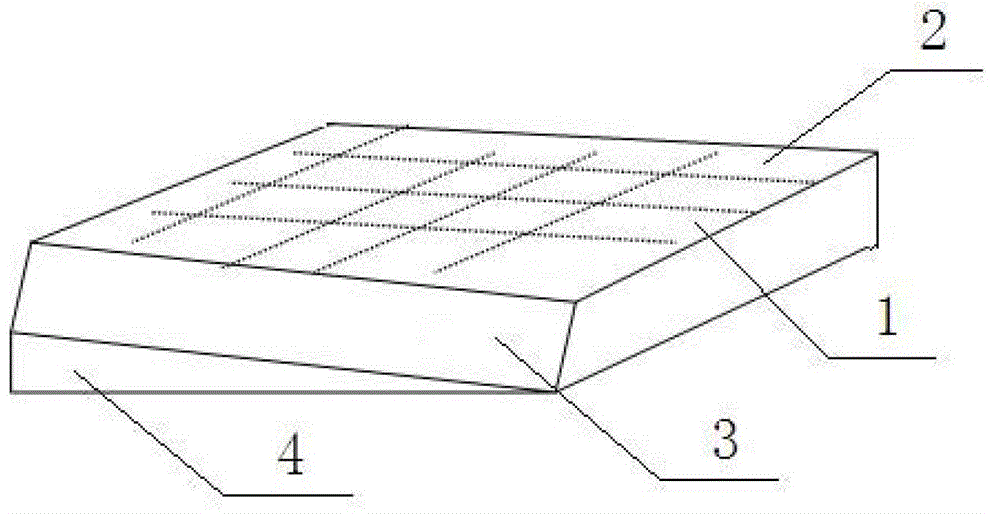
[0004] Different from this, in order to solve the same problem, the existing technology adopts the route of processing the chip body of the optical isolator, and processes the chip body of the optical isolator into a rhombus to avoid the influence of reflected light on the light source, and usually The approach taken in the case is, if figure 1 As shown, the free-space optical isolator chip body 1 includes a first plane 2 as the incident surface of light and a second plane 3 perpendicular to the first plane, and a wedge 4 is added below the optical isolator chip body 1, but, Since the blade in this method does not cut vertically into the isolator chip body, it must be cut with a thick blade to ensure the success of the cut. However, a thick blade will result in a larger cutting groove, and the cutting groove has a greater impact on the optical isolator. The chip body causes a certain loss, which in turn reduces the utilization rate of raw materials

Method used


Image

  • Cutting method for free-space photoisolator chip body
  • Cutting method for free-space photoisolator chip body
  • Cutting method for free-space photoisolator chip body

Examples


Embodiment Construction

[0024] The present invention will be further described in detail below in conjunction with test examples and specific embodiments. However, it should not be understood that the scope of the above subject matter of the present invention is limited to the following embodiments, and all technologies realized based on the content of the present invention belong to the scope of the present invention.

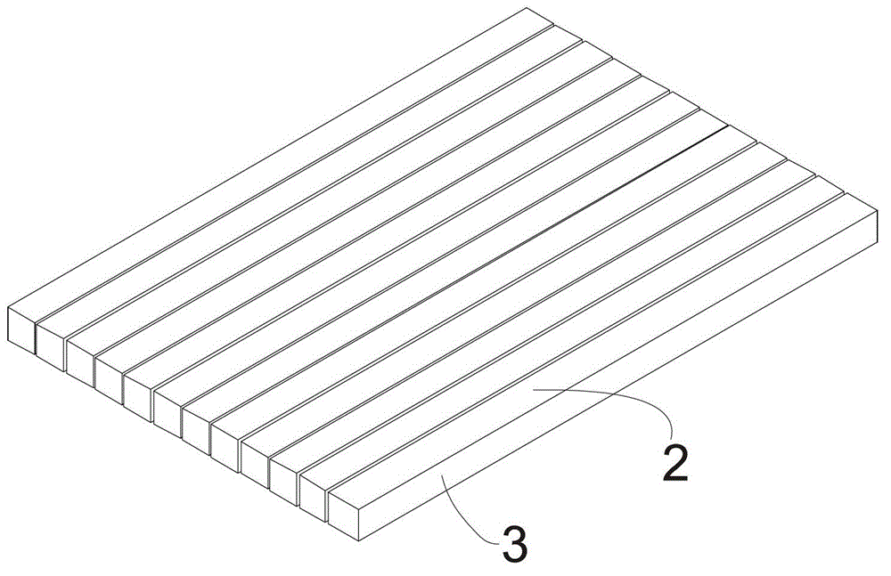
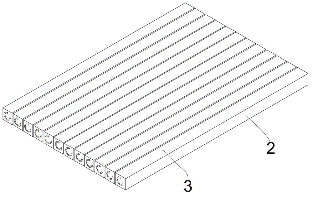
[0025] Such as Figures 2 to 5 Shown, a kind of cutting method of free space optical isolator chip body, the cutting method of described free space optical isolator chip is used for cutting free space optical isolator chip body, free space optical isolator chip body 1 includes as light incident The first plane 2 of the face and the second plane 3 perpendicular to the first plane comprise the following steps:

[0026] A. Set the first plane 2 horizontally upwards, cut the chip body of the free-space optical isolator along the same first cutting direction with a thin blade, and cu...


PUM


Abstract

The invention discloses a cutting method for a free-space photoisolator chip body. The free-space photoisolator chip body comprises a first plane as a light emitting surface of light and a second plane perpendicular to the first plane. The cutting method is characterized in that the cutting method comprises the following steps : A, cutting the chip body in the direction parallel to the second plane by using a blade and cutting the chip body into a plurality of chip strips; B, turning various chip strips into 90 degrees or 270 degrees by using long sides of the chip strips as axes; C, rotating each blade or each chip strip around the axis perpendicular to the second plane at an angle of 6 to 10 degrees; and D, cutting the chip strips in the direction perpendicular to the second plane by using the blade to form a plurality of rhombohedrons. According to the cutting method disclosed by the invention, the utilization rate of a photoisolator chip material can be effectively increased while the chip with low reflection of the photoisolator is obtained.

Description

technical field [0001] The invention relates to a processing method of an optical device, in particular to a cutting method of an optical isolator chip body. Background technique [0002] Semiconductor lasers are very sensitive to reflected light. When the intensity of reflected light reaches a certain level, it will cause instability in the work of the light source, resulting in frequency drift, amplitude changes, etc., which will affect the normal operation of the semiconductor laser. In order to avoid the reflected light from affecting the light source If the device is affected, an optical isolator must be used to suppress the reflected light to ensure the stable operation of the laser. [0003] In order to solve the above problems, most semiconductor lasers use an optical isolator to protect the laser, but the isolator itself will also bring reflections, so the Chinese invention patent application 201110185228.9 discloses that the first optical sheet in the optical isola...

Claims


Application Information

Patent Timeline
Patent Type & Authority Patents(China)
IPC IPC(8): B28D5/02
Inventor 叶磊
Owner SOURCE PHOTONICS CHENGDU
Learn More