Supercharge Your Innovation With Domain-Expert AI Agents!

Semiconductor devices with self-heating structures, methods of manufacture thereof, and testing methods

A self-heating, semiconductor technology, applied in the direction of single semiconductor device testing, semiconductor/solid-state device manufacturing, semiconductor/solid-state device testing/measurement, etc., can solve problems such as time-consuming

Active Publication Date: 2013-03-13
TAIWAN SEMICON MFG CO LTD
View PDF5 Cites 4 Cited by
  • Summary
  • Abstract
  • Description
  • Claims
  • Application Information

AI Technical Summary

Problems solved by technology

This requires the WAT team staff (team operator) to change the WAT probe card in the WAT tool and raise the temperature in the WAT tool to a higher temperature, which takes time

Method used


Image

  • Semiconductor devices with self-heating structures, methods of manufacture thereof, and testing methods
  • Semiconductor devices with self-heating structures, methods of manufacture thereof, and testing methods
  • Semiconductor devices with self-heating structures, methods of manufacture thereof, and testing methods

Examples


Embodiment Construction

[0035] The making and using of various embodiments of the invention are discussed in detail below. It should be appreciated, however, that the present invention provides many applicable inventive concepts that can be embodied in a wide variety of specific contexts. The specific embodiments discussed are merely illustrative of specific ways to make and use the invention, and do not limit the scope of the invention.

[0036] Embodiments of the invention relate to the fabrication of semiconductor devices and to the testing of semiconductor devices. Here, a semiconductor device having a built-in on-chip self-heating structure, its manufacturing method, and a testing method using the new self-heating structure will be described.

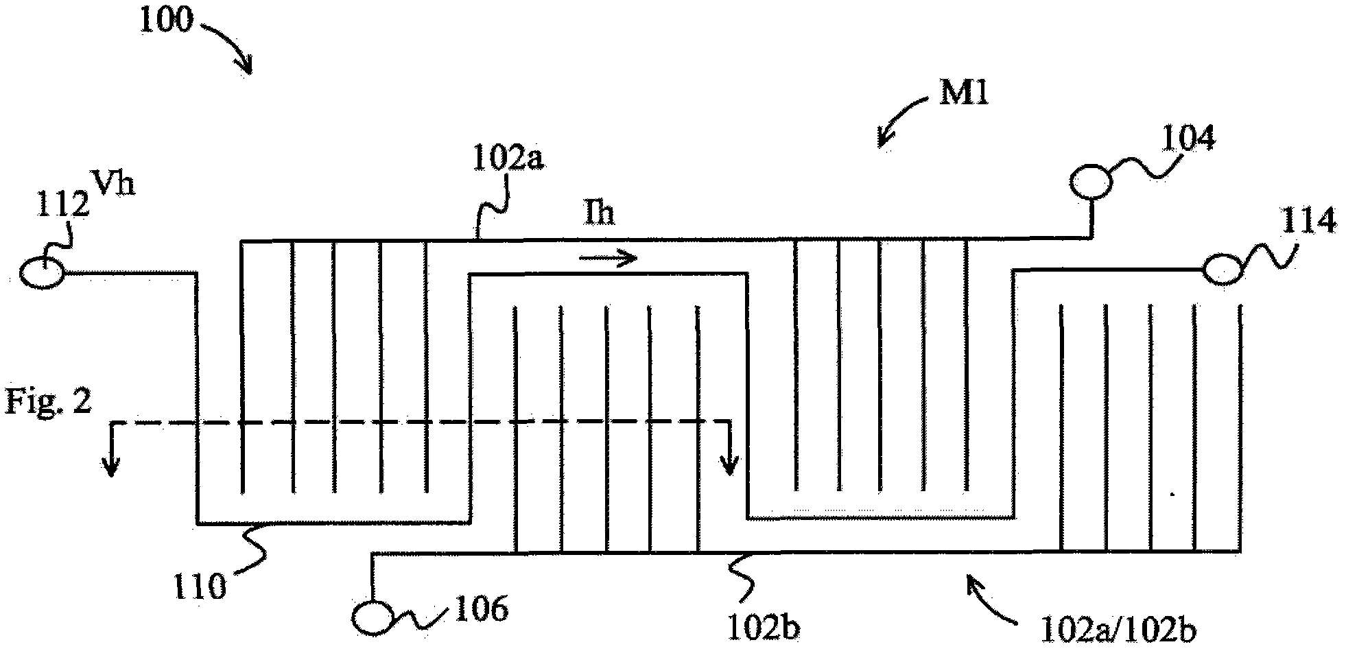
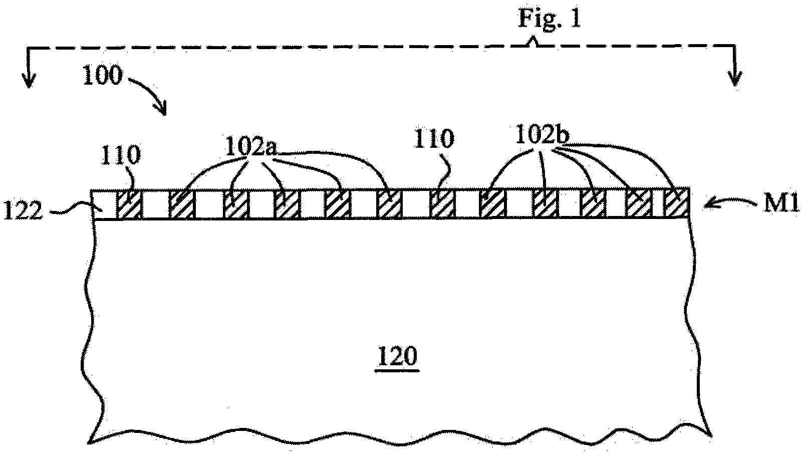
[0037] First, refer to figure 1 , shows a top view of the semiconductor device 100 including the active electrical structures 102a / 102b. For example, the term "active electrical structure" is used herein to describe structures that have active function...


PUM


Abstract

Semiconductor devices with self-heating structures, methods of manufacture thereof, and testing methods are disclosed. In one embodiment, a semiconductor device includes a workpiece, an active electrical structure disposed over the workpiece, and at least one self-heating structure disposed proximate the active electrical structure.

Description

technical field [0001] The present invention relates to a semiconductor device. Background technique [0002] Semiconductor devices can be used in various electronic applications such as personal computers, cell phones, digital cameras, and other electronic equipment. Semiconductor devices are typically fabricated by sequentially depositing insulating or dielectric layers, conductive layers, and semiconductor material layers over a semiconductor substrate and patterning the different material layers using photolithographic techniques to form circuit components and elements thereon. [0003] Metal Oxide Semiconductor (MOS) devices often require Wafer Acceptance Tests (WATs). For lifetime testing, part of the Wafer Acceptance Test involves heating the MOS device with an external circuit to test the operation of the wafer at elevated temperatures. Parameter (operating parameter). For example, semiconductor wafers sometimes require WAT at elevated temperatures for reliability ...

Claims


Application Information

Patent Timeline
IPC IPC(8): H01L23/544H01L21/66G01R31/26
CPCH01L22/34H01L23/345G06F19/00G01R31/2884G01R31/2875H01L23/5223G01R31/10H01L23/522H01L21/768H01L2924/0002H01L2924/00
Inventor 柯家洋邱盈翰王琳松
Owner TAIWAN SEMICON MFG CO LTD
Features
  • R&D
  • Intellectual Property
  • Life Sciences
  • Materials
  • Tech Scout
  • Unparalleled Data Quality
  • Higher Quality Content
  • 60% Fewer Hallucinations
Learn More