

Thin-film transistor, display part, manufacturing method of display part, and display device
A technology of thin film transistors and display devices, applied in the fields of display devices and their manufacturing methods, thin film transistors, and display devices, can solve the problems of increasing the complexity of the TFT hierarchical structure, increasing the manufacturing process and manufacturing costs, and saving process and cost , the effect of simplifying the hierarchy
- Summary
- Abstract
- Description
- Claims
- Application Information
AI Technical Summary
Problems solved by technology
Method used
Image

Examples
Embodiment 1
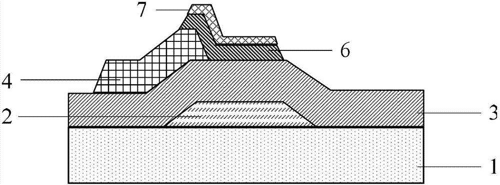
[0041] Such as figure 1 As shown, the thin film transistor TFT of this embodiment includes: a substrate 1 , a gate 2 , a gate insulating layer 3 , a drain 4 , a semiconductor connection portion 6 made of an oxide semiconductor material, and a source 7 . The gate 2 and the gate insulating layer 3 are sequentially formed on the substrate 1 (this embodiment uses a TFT with a bottom gate structure as an example for illustration).
[0042] Different from the traditional TFT structure, the source 7 and the drain 4 of the TFT in this embodiment are located in different layers, and are isolated by the semiconductor connection part 6 . Wherein, the semiconductor connecting portion 6 is located in the region corresponding to the gate 2 on the gate insulating layer 3, the drain 4 is located on the gate insulating layer 3, and is located on one side of the semiconductor connecting portion 6, and is in contact with the semiconductor connecting portion 6, and the source 7 Located above the...
Embodiment 2
[0046] This embodiment provides a display device adopting the TFT structure of Embodiment 1, and the display device may be an array substrate of a liquid crystal display or an array substrate of an AM-OLED structure. The following uses an array substrate of a liquid crystal display as an example for illustration. The array substrate may be similar to a traditional array substrate, and the entire TFT is arranged on one side of the gate line during fabrication. Due to the small volume of the TFT in Embodiment 1, in this embodiment, part of it is fabricated on the gate line, and the gate line is used as the gate, so that the aperture ratio of the array substrate can be increased.
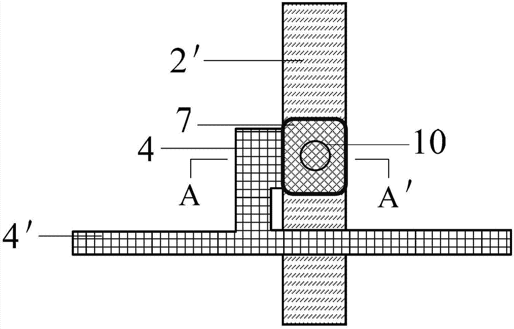
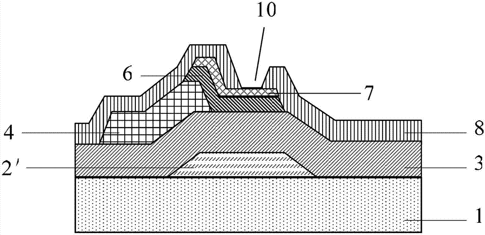
[0047] In this embodiment, the structure of the array substrate is as follows figure 2 with 3As shown, it includes: a substrate 1, a gate line 2', a data line 4'. The TFT of the above-mentioned embodiment 1 (including: a gate, a gate insulating layer 3, a drain 4, a semiconductor connection part 6 ma...
Embodiment 3
[0059] This embodiment provides a display device adopting the TFT structure of Embodiment 1, and the display device may be an array substrate of a liquid crystal display or an array substrate of an AM-OLED structure. In the following, the array substrate of a liquid crystal display is taken as an example for illustration. The difference between this array substrate and Embodiment 1 is that the entire TFT is fabricated on the gate line, and the gate line is used as the gate. Its structure is as follows: Figure 10 with 11 As shown, the area occupied by the drain 4, the source 7 and the semiconductor connection part 6 is located in the area of the gate line 2', that is, the drain 4, the source 7 and the semiconductor connection part 6 are all formed on the gate line. 2' above. The straight line in which the drain 4 , the source 7 and the semiconductor connecting portion 6 are arranged is parallel to the gate line 2 ′, and the drain 4 and the data line 4 ′ are integrally forme...
PUM
 Abstract
Description
Claims
Application Information