Directional coupler for photonic crystals

A technology of directional couplers and photonic crystals, applied in the field of couplers, can solve the problems of long coupling period, large volume, and low integration, and achieve the effects of small size, reduced device volume, and high integration

Active Publication Date: 2013-04-03
UNITED MICROELECTRONICS CENT CO LTD
View PDF5 Cites 9 Cited by
  • Summary
  • Abstract
  • Description
  • Claims
  • Application Information

AI Technical Summary

Problems solved by technology

However, the traditional photonic crystal directional coupler has a large volume and low integration due to its long coupling period.

Method used


Image

  • Directional coupler for photonic crystals
  • Directional coupler for photonic crystals
  • Directional coupler for photonic crystals

Examples


Embodiment Construction

[0027] In order to make the object, technical solution and advantages of the present invention clearer, the present invention will be further described in detail below in conjunction with the accompanying drawings and embodiments. It should be understood that the specific embodiments described here are only used to explain the present invention, not to limit the present invention.

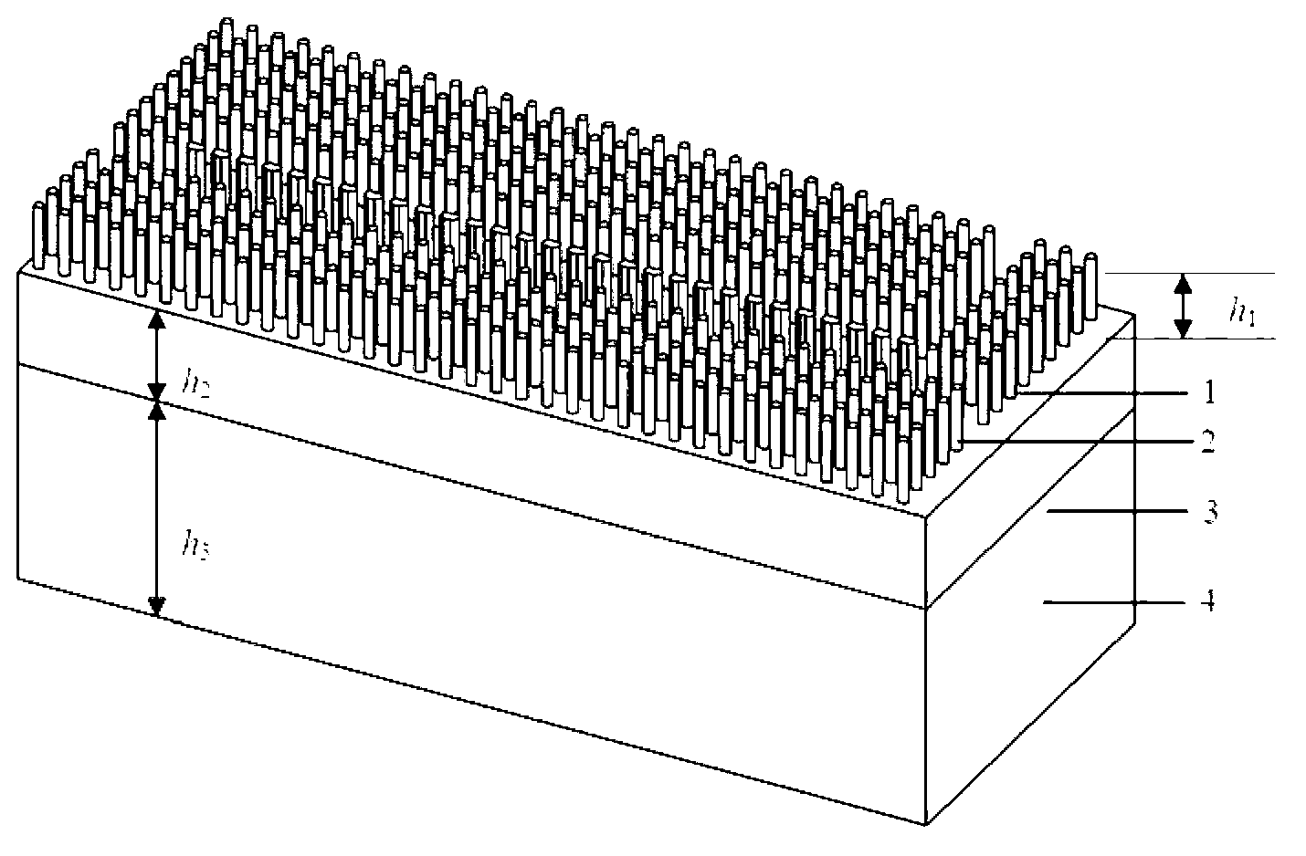
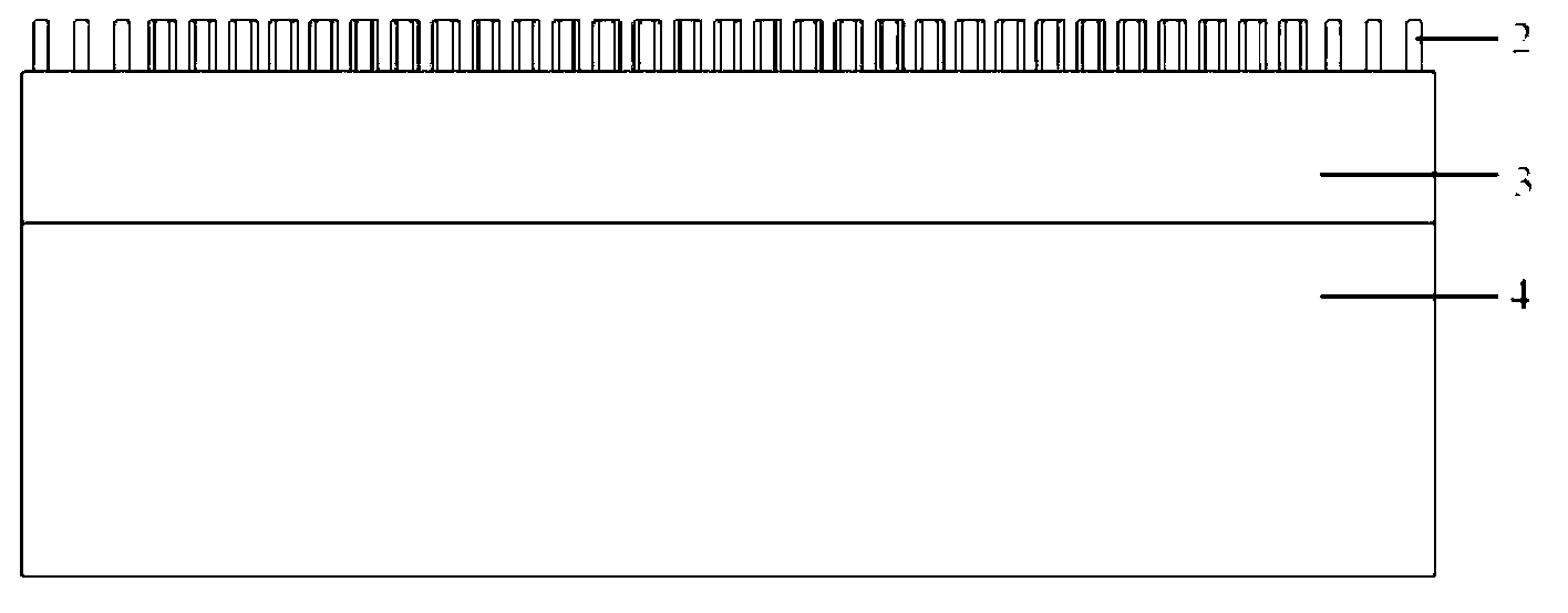
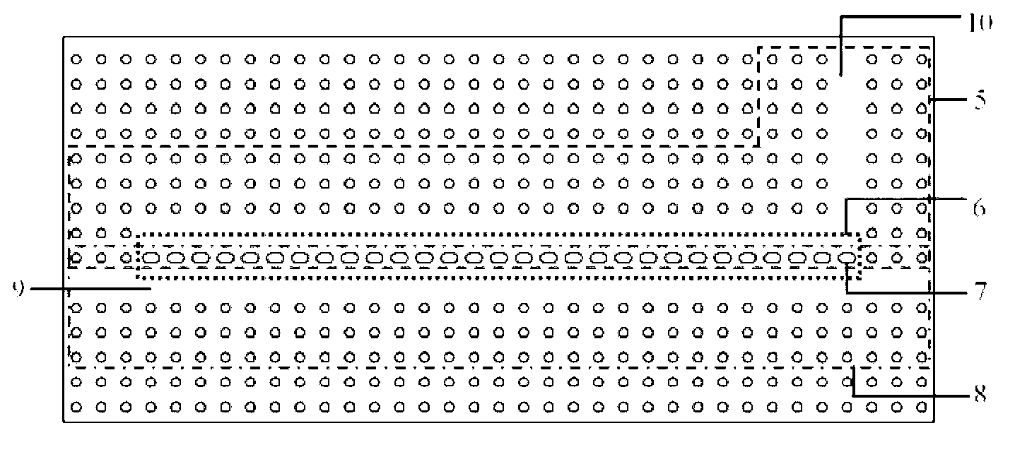
[0028] Such as figure 1 , 2 , 3 is a schematic structural diagram of a photonic crystal directional coupler provided by a preferred embodiment of the present invention. The photonic crystal directional coupler includes a substrate and a number of dielectric columns vertically arranged on the substrate. The plurality of dielectric columns surround two independent main waveguide defects 9 and coupling waveguide defects 10, and the main waveguide defect 9 and coupling waveguide There is a row of dielectric pillars between the line defects 10 , and the row of dielectric pillars are racetrack-shaped d...


PUM


Abstract

The invention discloses a directional coupler for photonic crystals. The directional coupler comprises a base board and a plurality of dielectric cylinders, wherein the dielectric cylinders are vertically arranged on the base board. A main waveguide line defect and a coupling waveguide line defect which are mutually independent are enclosed by the dielectric cylinders, at least one row of runway-shaped dielectric cylinders are spaced between the main waveguide line defect and the coupling waveguide line defect, and the rest dielectric cylinders are cylindrical. The directional coupler has the advantages that the coupling cycle of electromagnetic waves in the directional coupler is greatly shortened, so that the size of the coupler is reduced, the directional coupler is small in size, compact in structure, high in efficiency and integration level and the like, and an effective way for manufacturing a waveguide coupler and a wavelength division multiplexing device with smaller channel intervals on the fixed size is provided as the coupling cycle is shortened.

Description

technical field [0001] The invention relates to a coupler, in particular to a photonic crystal directional coupler. Background technique [0002] Photonic crystals, also known as optical semiconductors, are artificial microstructures formed by substances with different dielectric constants arranged periodically in space. Photonic crystals have a photonic band gap and have the characteristics of controlling the propagation of light in them. They are potential application materials for realizing large-scale optoelectronic integration and all-optical networks in the future. When defects are introduced in intact photonic crystal materials, defect states are introduced in the photonic forbidden band. For example, the introduction of point defects can localize the light in the defects to form a photonic crystal resonator; and if the introduction of line defects, the light can be confined to propagate in the line defects to form a photonic crystal waveguide. In recent years, opto...

Claims


Application Information

Patent Timeline
Patent Type & Authority Applications(China)
IPC IPC(8): G02B6/122
Inventor 崔乃迪郭进冯俊波滕婕王皖君周杰曹国威
Owner UNITED MICROELECTRONICS CENT CO LTD
Why Eureka
Try Eureka