
Device and method for overburden electroplating copper layer on chemical corrosion TSV (through silicon via) surface

A technology of chemical corrosion and electroplating of copper layer, applied in the manufacturing of circuits, electrical components, semiconductor/solid-state devices, etc., can solve the problems of excessive copper thickness on the surface, rising costs, raised crystals on the wafer surface, etc., to reduce the burden and reduce the cost effect

Active Publication Date: 2015-07-08
NAT CENT FOR ADVANCED PACKAGING CO LTD
View PDF3 Cites 0 Cited by
  • Summary
  • Abstract
  • Description
  • Claims
  • Application Information

AI Technical Summary

Problems solved by technology

Due to the influence of factors such as the ratio of various additives and time settings, the copper on the surface of the wafer after electroplating is over-plated, and the thickness of the copper layer on the surface varies. Moreover, because the cleanliness of the wafer surface cannot be completely guaranteed, the wafer with particle contamination , will cause additional raised crystallization on the wafer surface
These conditions will cause the surface copper after electroplating to be too thick, which will bring additional burden to the subsequent chemical mechanical polishing (CMP) process, which will not only increase the cost, but also bring challenges to the CMP process

Method used


Image

  • Device and method for overburden electroplating copper layer on chemical corrosion TSV (through silicon via) surface

Examples


Embodiment Construction

[0010] The present invention will be further described below in conjunction with drawings and embodiments.

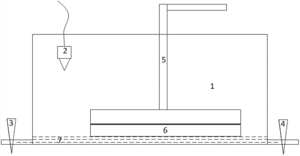
[0011] The main body of the device of the present invention is a simple copper corrosion tank 1, and a ranging sensor 2 is provided on the tank wall (ultrasonic ranging is selected here, and the precision is micron level), which is used to measure the liquid level in the tank. Liquid inlet and outlet, install inlet valve 3 and outlet valve 4 respectively; the wafer after TSV plating is held by an external mechanical arm 5, such as a lever or a mechanical arm, and the surface of the wafer (wafer) 6 is immersed in the copper corrosion tank 1 In the corrosive liquid 7 inside. Its diagram is as follows figure 1 shown. The controllers of the distance measuring sensor 2, the inlet valve 3, the outlet valve 4 and the mechanical arm bar 5 are all connected to a general controller or computer. The corrosion solution can be concentrated nitric acid (concentration 16mol / L-19mol...


PUM


Abstract

The invention provides a device and a method for an overburden electroplating copper layer on a chemical corrosion TSV (through silicon via) surface. The device comprises a distance measurement sensor, a corrosive liquid inlet and a corrosive liquid outlet. The distance measurement sensor is arranged in a copper corrosion groove and is used for measuring liquid level in the groove, and the corrosive liquid inlet and outlet are arranged at the bottom of the copper corrosion groove and are used for mounting an inlet valve and an outlet valve respectively. The device further comprises a mechanical arm rod for holding a wafer and soaking the surface of the wafer subjected to TSV electroplating in corrosive liquid in the copper corrosion groove. The distance measurement sensor, the inlet valve, the outlet valve and a controller for the mechanical arm rod are all connected to a master controller or computer. The device and the method for the overburden electroplating copper layer on the chemical corrosion TSV surface have the advantages that based on the thought of removing a superficial over-thick copper layer by combining chemical corrosion copper with the CMP (chemical mechanical polishing) process, a simple device for etching copper by a chemical wet method is designed. The problem of TSV overburden electroplating can be solved effectively, a majority of copper is removed by a method of wet-method corrosion copper to relieve load for the CMP copper process, and cost is reduced.

Description

technical field [0001] The invention relates to a device and method for chemically corroding an overelectroplated copper layer on a through-silicon hole surface, and belongs to the technical field of wafer-level electroplating copper hole filling. Background technique [0002] At present, TSV vertical interconnection technology has been more and more widely used in the field of microelectronic packaging, and TSV electroplating copper filling technology is an indispensable link in the TSV process. TSV electroplating and filling will inevitably cause copper overplating (overburden) on the surface of the wafer. ). Due to the influence of factors such as the ratio of various additives and time settings, the copper on the surface of the wafer after electroplating is over-plated, and the thickness of the copper layer on the surface varies. Moreover, because the cleanliness of the wafer surface cannot be completely guaranteed, wafers with particle contamination , will cause additi...

Claims


Application Information

Patent Timeline
Patent Type & Authority Patents(China)
IPC IPC(8): H01L21/768
Inventor 于大全伍恒程万
Owner NAT CENT FOR ADVANCED PACKAGING CO LTD
Learn More