Electric leading-out structure of sensor chip to be detected and application thereof
A technology for a sensor to be tested and an extraction structure, which is applied in the directions of thermometers using electrical/magnetic components directly sensitive to heat, measurement and instruments using the property force of piezoelectric resistance materials, etc. Stress is absolutely and accurately measured, not zero, etc., to achieve the effect of real-time online measurement
Inactive Publication Date: 2013-04-03
SHANGHAI INST OF MICROSYSTEM & INFORMATION TECH CHINESE ACAD OF SCI
View PDF3 Cites 6 Cited by
- Summary
- Abstract
- Description
- Claims
- Application Information
AI Technical Summary
Problems solved by technology
[0004] Generally speaking, the measured output of the stress sensor is linearly proportional to the stress in theory. Before the sensor is packaged, the output should be zero. However, due to the residual stress introduced by the sensor during the manufacturing process, and the influence of the test environment, especially the temperature It is very large, so that the test output before the sensor package is not zero, and the sensor output and the stress deviate from the linear proportional relationship. Therefore, the output of the test sensor chip before package and the temperature of the test chip are very important, which will affect the accuracy of package stress measurement. an important question of
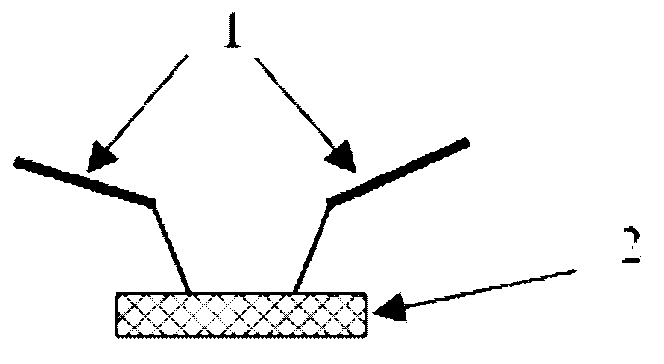
[0005] The conventional pre-value calibration method is generally obtained by pressing the probe to the pad of the chip to be tested, and then connecting the external measurement device through the metal bonding wire to measure the value after the sensor is packaged (Figure 1), Figure 1(a) It is a schematic diagram of the measurement of the previous value before the sensor is packaged. The probe 1 is pressed onto the test chip 2, and the other end of the probe is connected to an external test device
Method used
View moreImage
Smart ImageViewing Examples

Examples
 PUM
| Property | Measurement | Unit |
|---|---|---|
| Deposition thickness | aaaaa | aaaaa |
Abstract
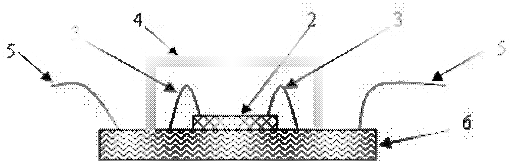
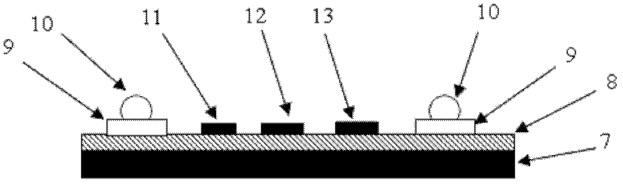
The invention relates to an electric leading-out structure of a sensor chip to be detected and an application thereof. The sensor chip (16) to be detected is provided with a pad (9) and a metal welding point (10) located on the pad (9). The electric leading-out structure further comprises a flexible substrate (14) provided with the pad and an interconnecting line. The sensor chip to be detected is reversely welded on the pad of the flexible substrate (14) through the welding point (10). Electric lead-out is realized through a welding line (15) by the pad of the flexible substrate (14). According to the invention, electric lead-out of a stress/temperature sensor is realized through the flexible substrate, and then the sensor with electric lead-out is used as an analog chip which is packaged by a packaging technique to be detected. The stress led in by the packaging technique can be obtained by measuring stress changes before and after packaging. The method of electric lead-out through the flexible substrate solves the problem that the stress sensor for packaging is hard to calibrate before packaging. The sensor is further used to measure the packaging stress and temperature in real time online.
Description
technical field [0001] The invention belongs to the technical field of integrated circuit manufacturing, packaging and measurement. Specifically, it refers to the electrical lead-out structure of the sensor chip to be tested and its application. Background technique [0002] With the development of integrated circuit packaging technology in the direction of miniaturization, high density and three-dimensional packaging, and the continuous increase of chip area, the problem of chip stress caused by packaging has become increasingly prominent and has become one of the main reasons for device failure. Therefore, testing and analyzing packaging stress has become an important link to improve packaging technology and device reliability. Compared with the traditional stress test method, the stress test chip manufactured by using the piezoresistive effect of silicon is compatible with conventional integrated circuit technology, the measurement equipment is relatively simple, and the...
Claims
Login to view more Application Information
Patent Timeline
 IPC IPC(8): H01L23/488G01L1/18G01K7/18H01L21/66
CPCH01L2224/10H01L2224/48091H01L2924/00014
Inventor 杨恒豆传国吴燕红李昕欣王跃林
Owner SHANGHAI INST OF MICROSYSTEM & INFORMATION TECH CHINESE ACAD OF SCI
- R&D Engineer
- R&D Manager
- IP Professional
Why Eureka
- Industry Leading Data Capabilities
- Powerful AI technology
- Patent DNA Extraction
Try Eureka
Browse by: Latest US Patents, China's latest patents, Technical Efficacy Thesaurus, Application Domain, Technology Topic.
© 2024 PatSnap. All rights reserved.Legal|Privacy policy|Modern Slavery Act Transparency Statement|Sitemap