Tunneling magneto-resistance multilayer film material

A technology of tunneling magnetoresistance and multi-layer film, applied in the direction of material selection, etc., can solve problems such as the adverse effect of spin polarizability magnetoresistance, and achieve good spin polarization performance, good mutual compatibility, and high spin pole. The effect of chemical performance

Inactive Publication Date: 2013-04-03
HEBEI UNIV OF TECH
View PDF4 Cites 0 Cited by
  • Summary
  • Abstract
  • Description
  • Claims
  • Application Information

AI Technical Summary

Problems solved by technology

[0004] The technical problem to be solved by the present invention is to provide a tunneling magnetoresistance multilayer film material (CoTiSb) with a high spin polarizability interface x / Fe y / (CoTiSb) z TMR multilayer film material with superlattice structure, the highest spin polarizability of the interface in this series of materials can reach 100%, and when the Fe atomic layer has defects, the material can still maintain a high spin polarizability, It overcomes the defect that in the prior art, the mismatch of the multilayer film interface of the practically applied TMR material and the mismatch of the electronic structure of different interlayer materials will have an adverse effect on the actual spin polarizability and magnetoresistance of the material

Method used


Image

  • Tunneling magneto-resistance multilayer film material
  • Tunneling magneto-resistance multilayer film material
  • Tunneling magneto-resistance multilayer film material

Examples


Embodiment 1

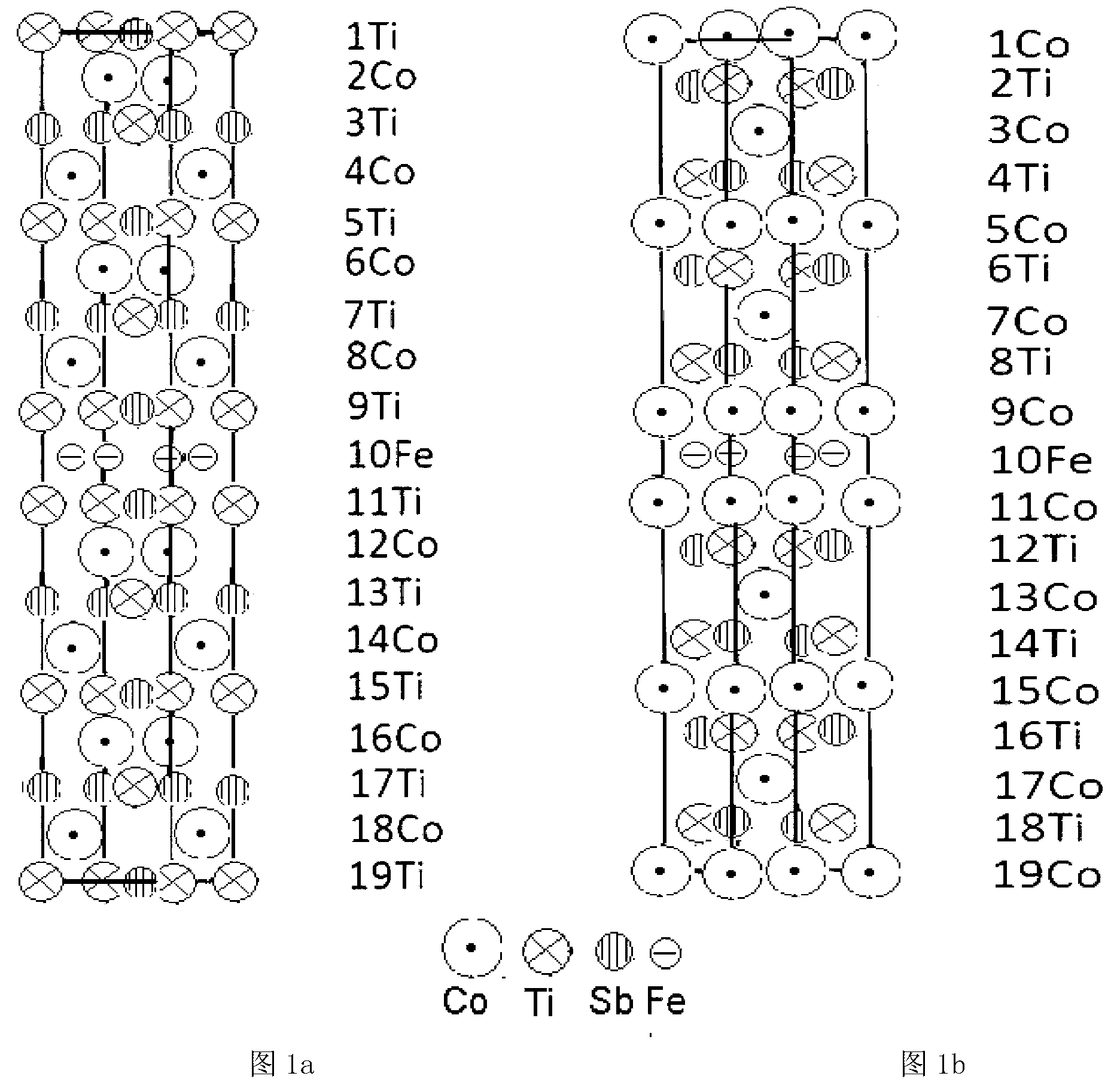
[0024] Preparation of (CoTiSb) with 1 Fe atomic layer and Fe-Co interface and Fe-TiSb interface 5 / Fe 1 / (CoTiSb) 5 TMR multilayer film material with superlattice structure.

[0025] The CoTiSb single crystal is prepared by pulling method. In order to obtain the Fe-Co interface and the Fe-TiSb interface, a layer of Co or TiSb atomic layer and a layer of Fe atoms are grown sequentially on the CoTiSb single crystal sample by molecular beam epitaxy. layer, and then grow a Co layer or TiSb layer on the Fe atomic layer, and then alternately grow a TiSb layer or Co layer, so that a CoTiSb with a Fe-Co interface and a Fe-TiSb interface with a Fe atomic layer is prepared. TMR multilayer film material with / Fe / CoTiSb superlattice structure. The specific process is as follows:

[0026] The first step, CoTiSb single crystal pulling

[0027] The cooling water outlet temperature is stable within the range of 25±10°C, and the vacuum pressure is not greater than 6×10 during the whole pr...

Embodiment 2

[0052] Preparation of (CoTiSb) with two Fe atomic layers and Fe-Co interface and Fe-TiSb interface 10 / Fe 2 / (CoTiSb) 10 TMR multilayer film material with superlattice structure.

[0053] The difference from Example 1 is that a Co-Fe-TiSb interface is produced when there are two layers of Fe atomic layers. In the actual growth process, a layer of Co is first grown on the CoTiSb single crystal by molecular beam epitaxy. Then grow two Fe atomic layers on the Co layer. The thickness of the Fe atomic layer is 0.29nm. The annealing time of step (9) in Example 1 is extended to 3 hours, and then alternately grow TiSb layers and Co on the Fe atomic layer. Layer, the thickness of the grown CoTiSb atomic layer is controlled to be 1nm, thereby growing a CoTiSb / Fe / CoTiSb film comprising two Fe atomic layers with a Co-Fe-TiSb interface, and other processes are the same as in Example 1.

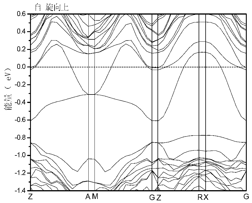
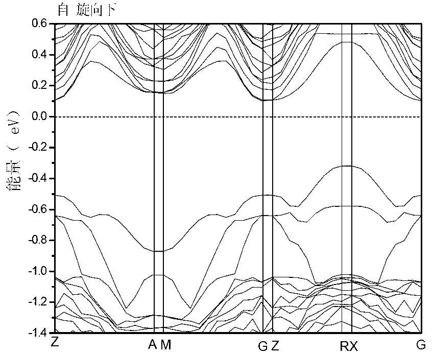
[0054] TMR of a CoTiSb / Fe / CoTiSb superlattice structure with 2 layers of Fe atomic layers and Fe-Co ...

Embodiment 3

[0057] Preparation of (CoTiSb) with 3 Fe atomic layers and Fe-Co interface and Fe-TiSb interface 15 / Fe 3 / (CoTiSb) 15 TMR multilayer film material with superlattice structure.

[0058] The difference from Example 1 is: the thickness of the Fe atomic layer is three atomic layers, and the thickness is 0.435nm. In real-time observation, when the Fe atomic layer reaches a thickness of three atomic layers, the thickness of the grown CoTiSb atomic layer is 1.5nm. The annealing time of step (9) in Example 1 was extended to 4 hours. Using this method, a multilayer film material with a high spin polarizability greater than 90% at both the Fe-TiSb interface and the Fe-Co interface was obtained. The other processes were the same as Example 1.


PUM

PropertyMeasurementUnit
Thicknessaaaaaaaaaa
Thicknessaaaaaaaaaa
Thicknessaaaaaaaaaa

Abstract

The invention relates to static memories applying multiple magnetic layers, in particular to a tunneling magneto-resistance multilayer film material. The TMR (tunneling magneto-resistance) multilayer film material is of a high-spin polarizability interface (CoTiSb)x / Fey / (CoTiSb)z superlattice structure, wherein the x, the y and the z refer to the atom layer number of each component, the superlattice structure is a multilayer film structure which grows coherently along the direction of a semi-Heusler structure CoTiSb single crystal [100] by taking a three-layer film as a basic unit and is capable of achieving periodic epitaxy by taking the basic unit as a base, and in an inserted Fe layer and a high-spin polarization layer induced by the same, a few vacancy or island-shaped defects cannot have a great influence on high-spin polarizability. The tunneling magneto-resistance multilayer film material overcomes the defect that unmatching of multilayer film interfaces of a TMR material in practical use and unmatching of electronic structures of different interlayer materials can have adverse influences on practical spin polarizability and magneto-resistance in the prior art.

Description

technical field [0001] The technical scheme of the invention relates to a static memory using multilayer magnetic layers, in particular a tunnel magnetoresistance multilayer film material. Background technique [0002] Magnetoresistive materials are widely used in the fields of high-density readout heads, magnetic sensors, weak magnetic field measurement and detection of various motions, thus becoming a research field attracting international attention. After using the GMR read head, the recording density of the computer hard disk is increased by nearly 500 times. In recent years, the tunneling magnetoresistance (hereinafter referred to as TMR) effect with MgO as the insulating layer has made a breakthrough. The performance of the magnetic sensor prepared with it has significantly exceeded that of the GMR effect device, and it has also entered the commercial field in the field of readout heads. stage. The typical application of TMR is on magnetic random access memory (here...

Claims


Application Information

Patent Timeline
IPC IPC(8): H01L43/10
Inventor 王立英代学芳刘国栋贾红英
Owner HEBEI UNIV OF TECH
Why Eureka
Try Eureka