

A kind of atomic layer deposition equipment and using method thereof
A technology of atomic layer deposition and equipment, which is applied in the direction of coating, metal material coating process, gaseous chemical plating, etc., can solve the problem that atomic layer deposition equipment is difficult to meet the application requirements, can not meet the fine requirements of device thickness, and the film layer is uniform In order to improve the film thickness control ability, reduce the drift of film layer thickness and meet the requirements of refinement
Active Publication Date: 2016-01-20
INST OF MICROELECTRONICS CHINESE ACAD OF SCI
View PDF8 Cites 0 Cited by
- Summary
- Abstract
- Description
- Claims
- Application Information
AI Technical Summary
Problems solved by technology
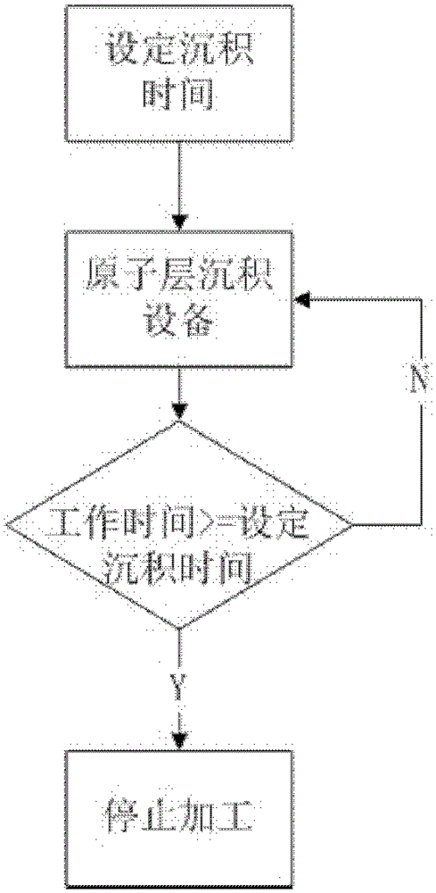
The existing atomic layer deposition equipment controls the thickness of the film layer by preset deposition reaction time. Although the film thickness can be accurately controlled in theory, in the actual production process, it is often due to the degree of contamination of the device to be processed. As well as the purity of the gas phase precursor, the uniformity of the film layer is not good, and there is a certain amount of drift in the thickness
Therefore, controlling the thickness of the film layer by setting the reaction time can no longer meet the fine requirements of modern semiconductor technology for device thickness.
Relying only on the calculated reaction time or the staff's estimation of the reaction time, it is difficult for the traditional atomic layer deposition equipment to meet the application requirements when the film thickness and uniformity are required to be extremely precise.
Method used
View moreImage
Smart ImageViewing Examples

Examples
Embodiment Construction
[0027] The technical solution of the present invention will be described in detail below in conjunction with the accompanying drawings and embodiments.
Login to View More PUM
 Abstract
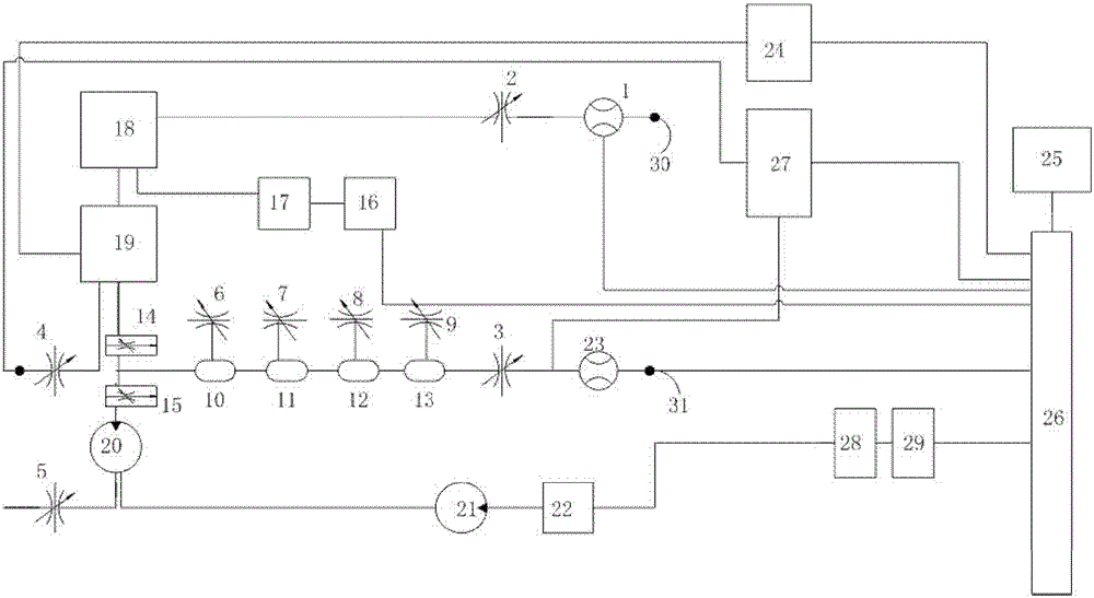
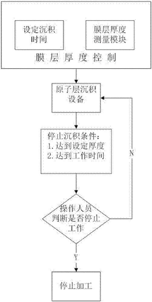
The invention relates to the technical field of manufacturing of a semiconductor, in particular to atomic layer deposition equipment. The atomic layer deposition equipment comprises a vacuum component, a heating component, an airway component, a plasma generation component, a control component and a deposition chamber, wherein a film thickness measuring module is arranged in the deposition chamber; and the film thickness measuring module is electrically connected with the control component. The invention also provides a use method of the atomic layer deposition equipment. Through the adoption of the deposition time and the film thickness measuring module, the atomic layer deposition equipment and the use method thereof cause the film thickness control capability of the atomic layer deposition equipment to be improved and the equipment faults to be decreased; and therefore, a processed film is enabled to approach a required thickness more closely, the thickness drift of the film is effectively decreased, the equipment utilization rate is improved, and moreover, the requirement on finer and finer semiconductor processing can be met.
Description
technical field [0001] The invention relates to the technical field of semiconductor manufacturing, in particular to an atomic layer deposition device and a method for using the same. Background technique [0002] The working steps of traditional atomic layer deposition equipment are generally as follows: the thickness of the film required by the device to be processed is known, before the deposition work starts, the required reaction time and the volume of the gas to be fed are calculated, and the control valve is opened to feed the precursor gas to the preset value. amount, close the valve, and proceed to the reaction. After the reaction time reaches the preset amount, the deposition is stopped, and the cleaning gas is introduced to clean the gas circuit system and deposition chamber of the equipment. That is, during the working process of the equipment, the deposition reaction process is controlled by the preset time, and the setting of the time depends on the experience...
Claims
Login to View More Application Information
Patent Timeline
 Patent Type & AuthorityPatents(China)
IPC IPC(8): C23C16/52
Inventor王燕李勇滔夏洋赵章琰石莎莉
OwnerINST OF MICROELECTRONICS CHINESE ACAD OF SCI