Semiconductor laser component

A technology of laser components and semiconductors, applied in semiconductor lasers, laser parts, lasers, etc., can solve the problems of unstable film thickness, poor reproducibility, and poor effective refractive index of the refractive index control layer 9, and achieve improved film thickness control Excellent reproducibility and high manufacturing yield

Inactive Publication Date: 2006-06-14
MITSUI CHEM INC
View PDF1 Cites 0 Cited by
  • Summary
  • Abstract
  • Description
  • Claims
  • Application Information

AI Technical Summary

Problems solved by technology

Therefore, the film thickness of the refractive index control layer 9 becomes unstable due to the occurrence of a dwell time, etc., and as a result, there is a problem that the reproducibility of the effective refractive index difference in the width direction of the ribbon window R1 is poor.

Method used


Image

  • Semiconductor laser component
  • Semiconductor laser component
  • Semiconductor laser component

Examples


Embodiment Construction

[0023] Hereinafter, preferred embodiments of the present invention will be described in detail with reference to the accompanying drawings.

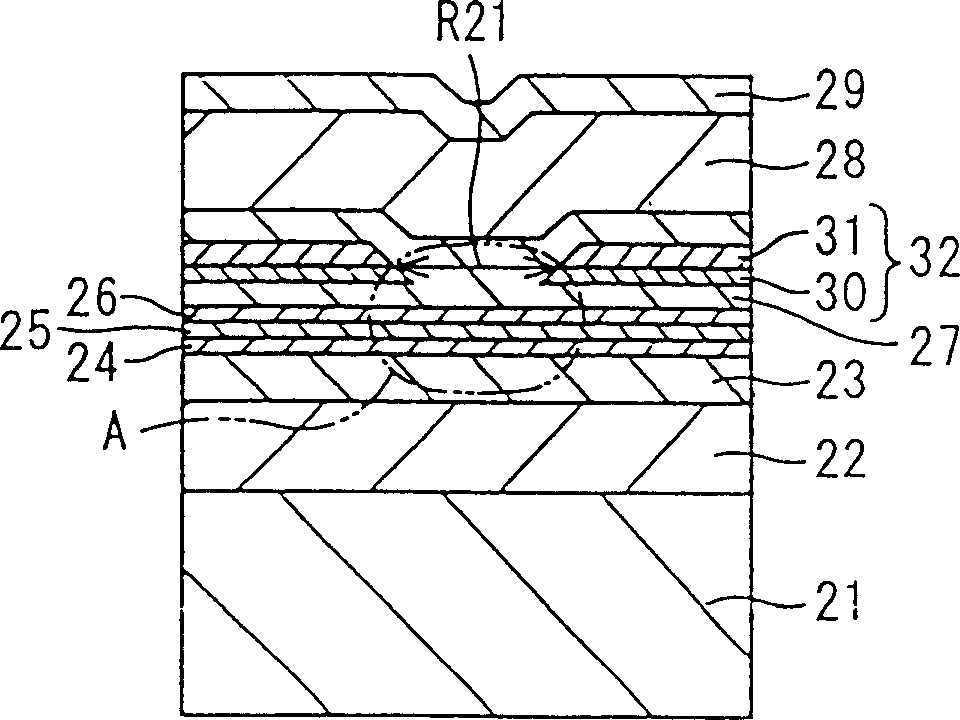
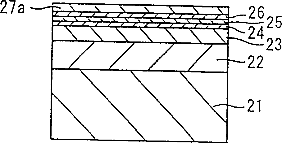
[0024] figure 1 It is a cross-sectional view showing the structure of a semiconductor laser element according to an embodiment of the present invention. In this embodiment, a DCH-SAS laser element using a semiconductor buffer layer is taken as an example for description. The semiconductor laser element is made of n-type Al on the n-type GaAs substrate 21. 0.09 Ga 0.91 As cladding layer 22, n-type GaAs optical waveguide layer 23, n-type Al 0.40 Ga 0.60 As carrier blocking layer 24, In 0.18 Ga 0.82 As / GaAs quantum well active layer 25, p-type Al 0.40 Ga 0.60 As carrier blocking layer 26, p-type GaAs optical waveguide layer 27, p-type Al 0.09 Ga 0.91 The As cladding layer 28 and the p-type GaAs contact layer 29 are stacked in this order.

[0025] In the semiconductor laser element, the light emitted from the active layer 25 is e...


PUM


Abstract

It is an object of the present invention to provide a semiconductor laser element having high film thickness controllability of a selectively grown refractive index control layer, good reproducibility of effective refractive index difference, and high manufacturing yield. At least one side of the active layer (25) is provided with an optical waveguide layer (27) having a forbidden band width greater than the forbidden band width of the active layer (25), and an optical waveguide layer (27) is provided outside the optical waveguide layer (27). The cladding layer (28) with the forbidden band width above the forbidden band width is set on the optical waveguide layer (27), and the actual refractive index control layer (31) having a band window (R21) embedded through selective growth is set. In the refractive index waveguide type semiconductor laser element, the film thickness of the refractive index control layer is below 300nm, and the refractive index control layer (31) is embedded in the optical waveguide layer (27); For the semiconductor layer (30) which is selectively grown in advance, in the lamination part including the semiconductor layer (30) and the refractive index control layer (31), the change amount of the effective refractive index caused by the film thickness change of the semiconductor layer (30) is more than The change amount of the effective refractive index due to the film thickness change of the refractive index control layer (31) is smaller.

Description

technical field [0001] The present invention relates to an actual refractive index waveguide type semiconductor laser element capable of high-output operation, which is preferably used in communications, laser printers, laser medical treatment, laser processing, and the like. Background technique [0002] 4A to 4C This is a cross-sectional view showing the structure of an actual refractive index waveguide type semiconductor laser element (hereinafter referred to as DCH-SAS type LD) having a completely separated and closed structure as described in, for example, Japanese Patent Application Laid-Open No. 11-154775, and a manufacturing method thereof. [0003] exist Figure 4A On the n-type GaAs substrate 1, through sequential crystal growth, an n-type AlGaAs cladding layer 2, an n-type AlGaAs optical waveguide layer 3, an n-type AlGaAs carrier blocking layer 4, a GaAs / AlGaAs quantum well active layer 5, A part of the p-type AlGaAs carrier blocking layer 6 and the p-type AlGa...

Claims


Application Information

Patent Timeline
Patent Type & Authority Patents(China)
IPC IPC(8): H01S5/00H01S5/20H01S5/22H01S5/223
CPCH01S5/2077H01S5/222H01S5/2231
Inventor 藤本毅室清文小矶武
Owner MITSUI CHEM INC
Why Eureka
Try Eureka