Constant current diode formed by grooving process and its manufacturing method

A technology of constant current diode and manufacturing method, applied in semiconductor/solid-state device manufacturing, electrical components, circuits, etc., can solve the problem that current density and constant current characteristics cannot be taken into account at the same time, and achieve small reverse leakage, large current density, cost reduction effect

Active Publication Date: 2016-01-20
HANGZHOU SILAN INTEGRATED CIRCUIT +1
View PDF6 Cites 0 Cited by
  • Summary
  • Abstract
  • Description
  • Claims
  • Application Information

AI Technical Summary

Problems solved by technology

[0005] The object of the present invention is to provide a constant current diode formed by groove cutting process and its manufacturing method, so as to solve the problem that the current density per unit area and the constant current characteristic cannot be taken into account at the same time

Method used


Image

  • Constant current diode formed by grooving process and its manufacturing method
  • Constant current diode formed by grooving process and its manufacturing method
  • Constant current diode formed by grooving process and its manufacturing method

Examples


Embodiment Construction

[0043] In order to make the above objects, features and advantages of the present invention more comprehensible, specific implementations of the present invention will be described in detail below in conjunction with the accompanying drawings.

[0044] In the following description, numerous specific details are set forth in order to provide a thorough understanding of the present invention. However, the present invention can be implemented in many other ways different from those described here, and those skilled in the art can make similar extensions without violating the connotation of the present invention, so the present invention is not limited by the specific implementations disclosed below.

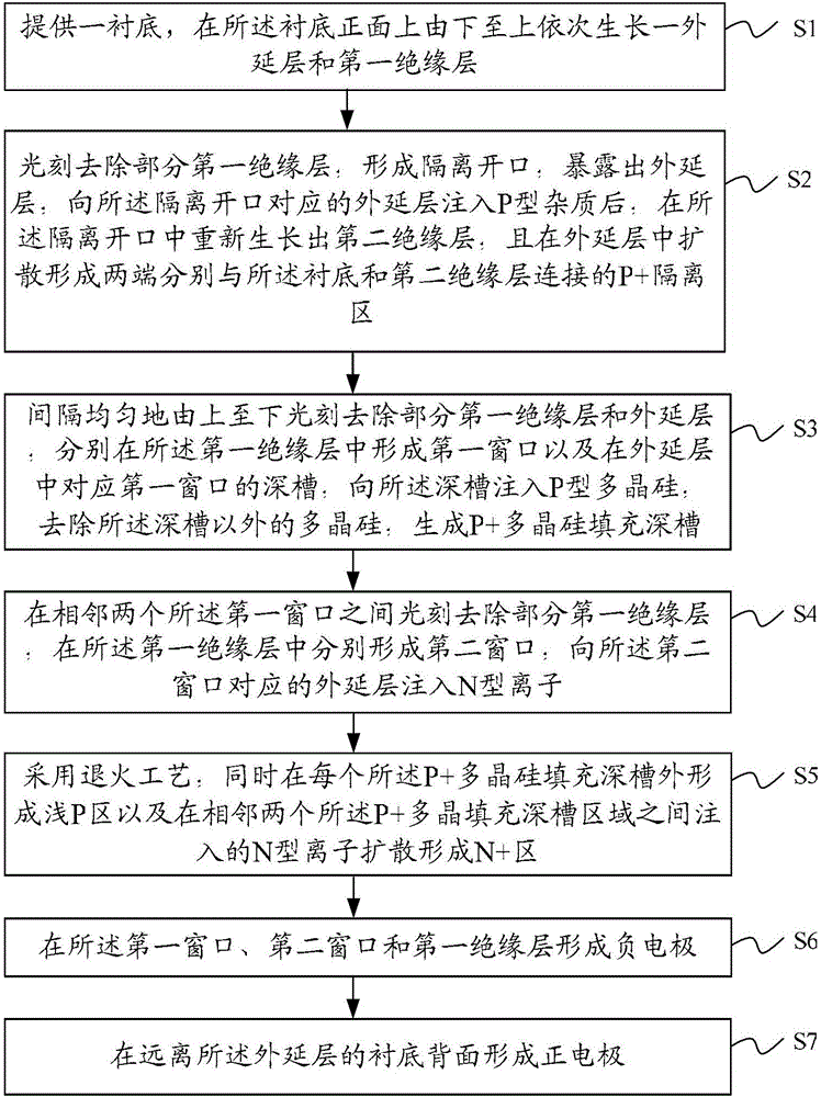
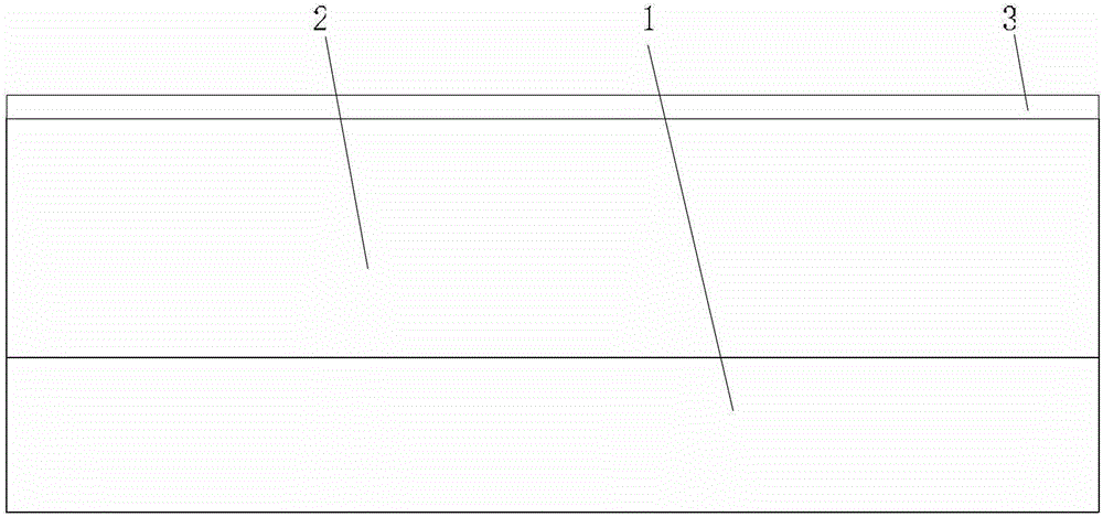
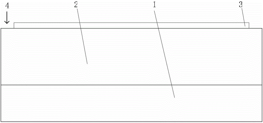
[0045] figure 1 For the process flow of a method for manufacturing a constant current diode formed by a groove-cutting process provided by the present invention, see figure 1 , combined with figure 2 Referring to FIG. 1 , the manufacturing process of a method for manufacturing a ...


PUM


Abstract

The invention provides a constant current diode formed by a grooving process. The constant current diode comprises a substrate, an epitaxial layer, a first insulating layer, a second insulating layer, a P+ isolation region, P+ polycrystalline silicon filled deep grooves, shallow P regions, a cathode and an anode, wherein the epitaxial layer is positioned on the front face of the substrate; the first insulating layer is provided with a first window and a second window and covers the surface of the epitaxial layer; the second insulating layer is adjacent to the first insulating layer and positioned on the surface of the epitaxial layer; the P+ isolation region is formed in the epitaxial layer and the two ends of the P+ isolation region are respectively connected with the substrate and the second insulating layer; the P+ polycrystalline silicon filled deep grooves are formed in the epitaxial layer corresponding to the first window; the shallow P region is formed outside each P+ polycrystalline silicon filled deep groove; the N+ region is positioned on the epitaxial layer corresponding to the second window and positioned between the two adjacent P+ polycrystalline silicon filled deep grooves; the cathode is positioned on the first window, the second window and the first insulating layer; and the anode is positioned on the back face of the substrate away from the epitaxial layer. The invention further provides a manufacturing method for the constant current diode formed by the grooving process, so as to solve the problem that current intensity per unit area and constant current characteristic cannot be simultaneously taken into account in the prior art.

Description

technical field [0001] The invention belongs to the technical field of semiconductor manufacturing technology, and in particular relates to a constant-current diode formed by a groove-cutting technology and a manufacturing method thereof. Background technique [0002] A constant current diode is a two-terminal constant current device made of silicon material. The constant current diode conducts forward to constant current and reverses to cut off. When the constant current diode is connected to the circuit loop according to the polarity and outputs a constant current when it is forward-conducting, the loop can achieve the effect of constant current, and the application is simple. Therefore, constant current diodes are widely used in electronic circuits such as AC and DC amplifiers, DC regulated power supplies, waveform generators, and protection circuits. [0003] Generally, the constant current diode adopts a planar channel junction field effect transistor (JFET) structure...

Claims


Application Information

Patent Timeline
Patent Type & Authority Patents(China)
IPC IPC(8): H01L29/861H01L29/06H01L21/329
Inventor 王英杰徐敏杰崔建
Owner HANGZHOU SILAN INTEGRATED CIRCUIT
Why Eureka
Try Eureka