Constant current diode and its manufacturing method

A technology of constant current diode and manufacturing method, applied in semiconductor/solid state device manufacturing, electrical components, circuits, etc., can solve the problem of poor uniformity of epitaxial thickness and concentration, affecting the yield of constant current diode 100, and resistance of N-type epitaxial layer 11 The problem of poor thickness uniformity of rate epitaxy, etc., achieves the effect of good constant current performance.

Active Publication Date: 2016-02-17
HANGZHOU SILAN INTEGRATED CIRCUIT
View PDF3 Cites 0 Cited by
  • Summary
  • Abstract
  • Description
  • Claims
  • Application Information

AI Technical Summary

Problems solved by technology

However, since the N-type epitaxial layer 11 is affected by the self-doping of the N-type substrate, the uniformity of the epitaxial thickness and concentration is relatively poor, so the resistivity of the N-type epitaxial layer 11 and the uniformity of the epitaxial thickness are relatively poor.
At the same time, due to the uneven resistivity of the epitaxial layer 11, the junction depth of the gate level 12 is uneven, resulting in poor uniformity of the constant current value, which affects the yield of the constant current diode 100.
[0005] It can be seen that the difference in the current value of the constant current diode 100 with the planar trench JFET structure is relatively large, so the yield of the product is relatively low.

Method used


Image

  • Constant current diode and its manufacturing method
  • Constant current diode and its manufacturing method
  • Constant current diode and its manufacturing method

Examples


preparation example Construction

[0049] According to the core idea of ​​the present invention, the present invention also provides a method for preparing a constant current diode, comprising the following steps:

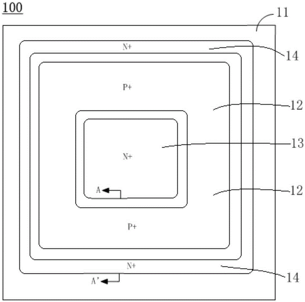
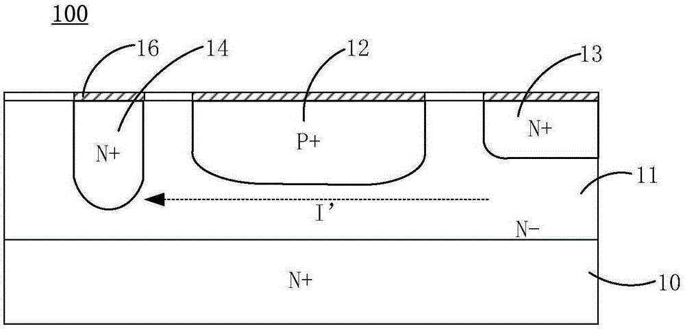
[0050] S10: providing a substrate;

[0051] S11: forming a first doped region on the substrate;

[0052] S12: forming an epitaxial layer on the surface of the first doped region and the substrate;

[0053] S13: forming a fourth doped region in the epitaxial layer;

[0054] S14: sequentially forming a second doped region and a third doped region in the epitaxial layer formed with the fourth doped region;

[0055] S15: forming a first positive electrode on the surface of the third doped region, and forming a second positive electrode on the surfaces of the second doped region and the fourth doped region;

[0056] S16: forming a negative electrode on the back surface of the substrate;


PUM


Abstract

The present invention provides a constant current diode, comprising: a substrate; an epitaxial layer formed on the substrate; a first doped region formed between the substrate and the epitaxial layer; formed on the epitaxial layer The second doped region, the third doped region and the fourth doped region; the first positive electrode formed on the surface of the third doped region and the first positive electrode formed on the surface of the second doped region and the fourth doped region The second positive electrode on the surface of the impurity region; the negative electrode formed on the back of the substrate; wherein, there are several first doped regions arranged side by side in the first direction between the third doped region and the fourth doped region. Two doped regions; the first doped region is in contact with the second doped region. The invention also provides a manufacturing method of the constant current diode. In the constant current diode and its manufacturing method provided by the present invention, a constant current diode with side gate plus bottom gate JFET structure is formed, its constant current value mainly depends on the distance between the second doped regions, and its constant current performance is good.

Description

technical field [0001] The invention relates to the technical field of semiconductors, in particular to a constant current diode and a manufacturing method thereof. Background technique [0002] A constant current diode (Current Regulative Diode, referred to as CRD) is a semiconductor constant current device that has come out in recent years. The forward conduction and reverse cutoff are the forward characteristics of the diode. Among them, the constant current diode has a constant current region when it works in the forward direction, and the output current in this region basically does not change with the voltage. The constant current diode has only two electrodes, so it is convenient to extend the current in parallel and extend the voltage in series. Due to its good constant current performance, simple structure, convenient use, and low cost, constant current diodes are widely used in LEDs, semiconductor lasers, and other occasions that require constant current power sup...

Claims


Application Information

Patent Timeline
Patent Type & Authority Patents(China)
IPC IPC(8): H01L29/861H01L29/06H01L21/329
CPCH01L29/0603H01L29/36H01L29/66121H01L29/8613
Inventor 王英杰徐敏杰崔建丁伯继
Owner HANGZHOU SILAN INTEGRATED CIRCUIT
Why Eureka
Try Eureka