Graphite die for sintering multichip

A graphite mold, multi-chip technology, applied in electrical components, semiconductor/solid-state device manufacturing, circuits, etc., can solve the problems of low sintering pass rate, inability to assemble and fix, collapse of multi-layer chips, etc., to achieve convenient use and simple structure. Effect

Inactive Publication Date: 2013-05-01
YIXING HUANZHOU MICRO ELECTRONICS
View PDF5 Cites 6 Cited by
  • Summary
  • Abstract
  • Description
  • Claims
  • Application Information

AI Technical Summary

Problems solved by technology

However, the assembly of multi-chips cannot be assembled and fixed by traditional graphite molds. Generally, graphite molds cannot play the role of fixing the position of chips in the assembly of multi-layer chips, and the assembly process is quite difficult, which may easily cause multi-layer chips in the assembly process. Collapse in middle and lead to low sintering pass rate

Method used


Image

  • Graphite die for sintering multichip
  • Graphite die for sintering multichip
  • Graphite die for sintering multichip

Examples


Embodiment 1

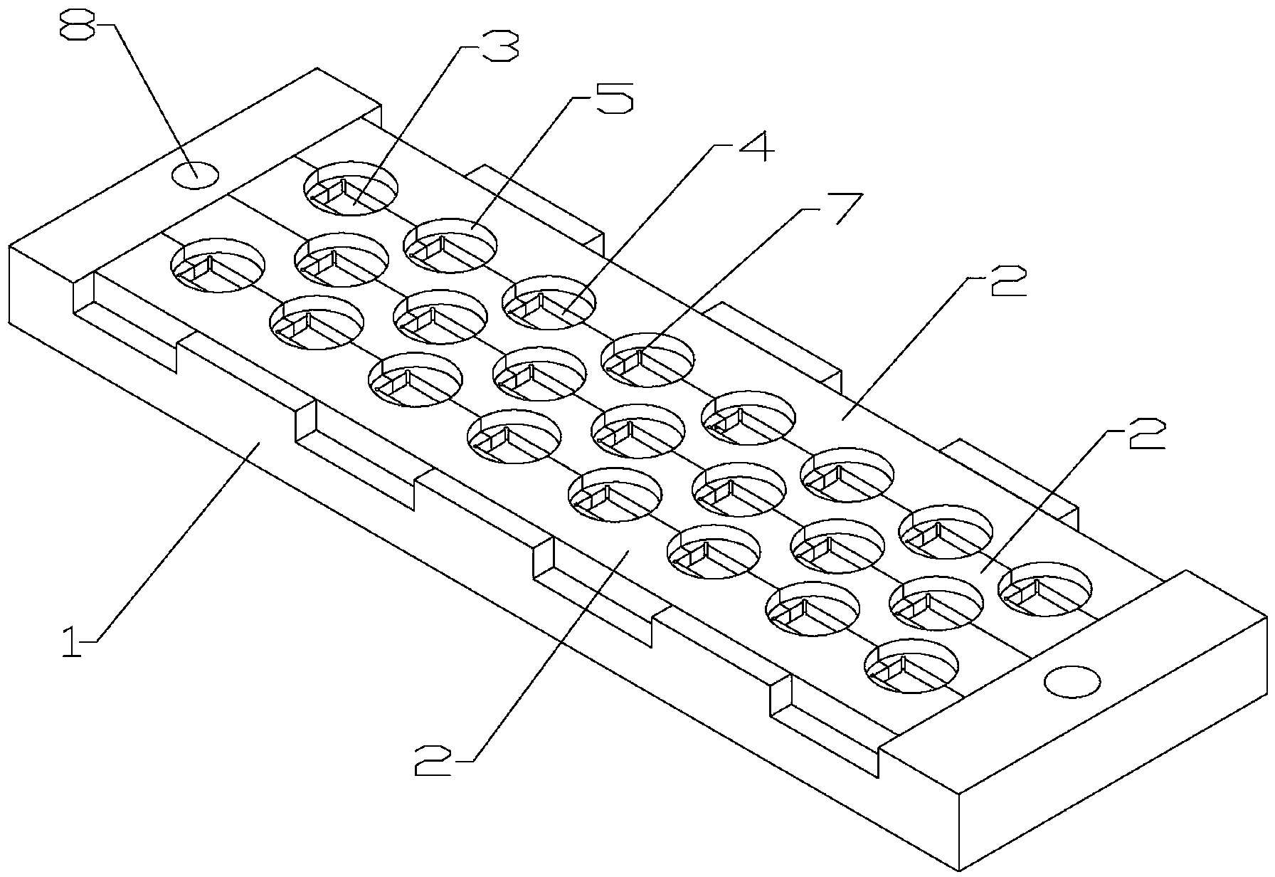
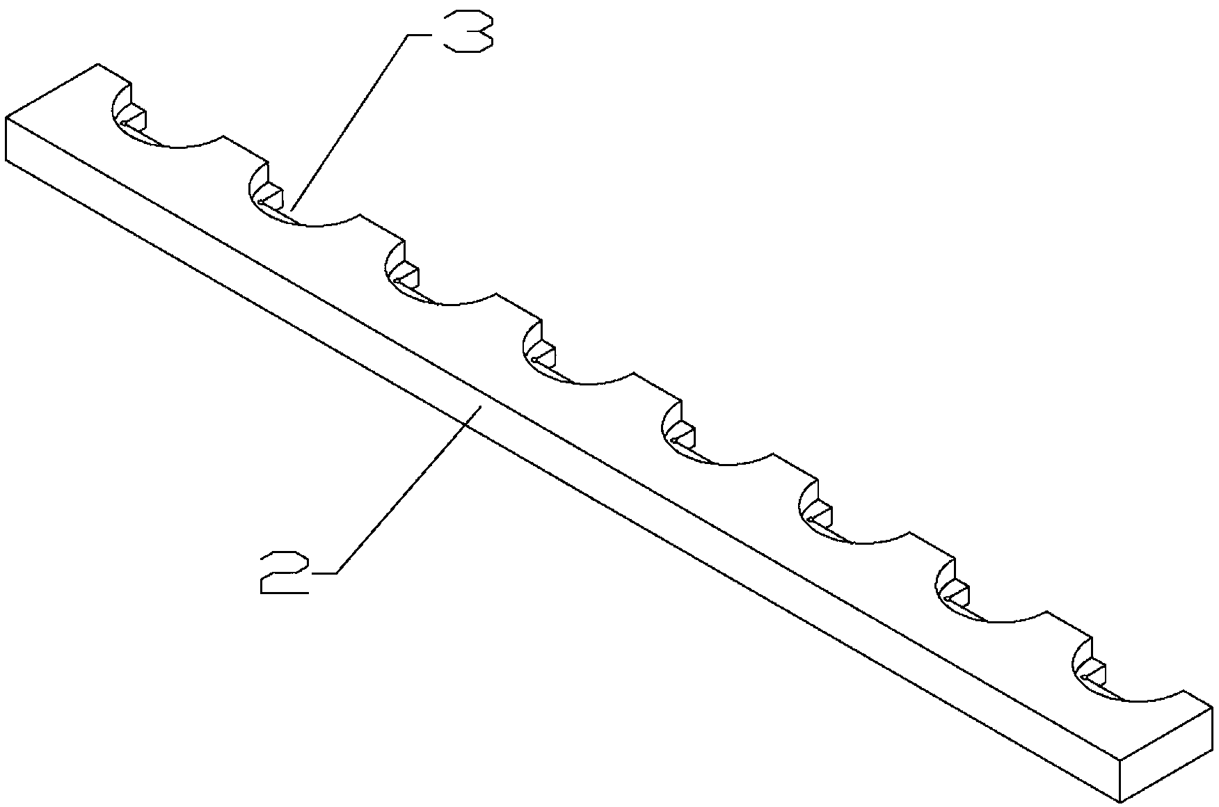
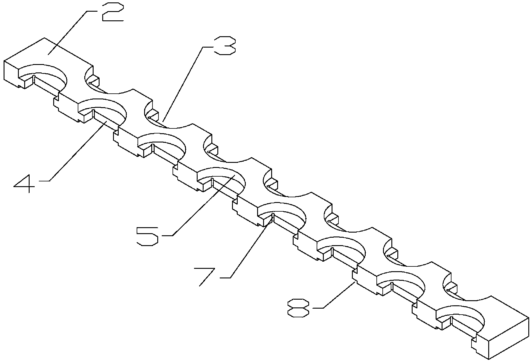
[0028] When the graphite mold of the present invention is in use, first a graphite assembly bar 2 with only one side provided with a sintering tank 3 is installed on the graphite base plate 1, then the bottom electrode is put into the lower sintering tank 6 of the graphite assembly bar 2, and then according to The first row of bottom electrodes line up the second graphite assembly bar 2; then put the bottom soldering sheet at the bottom of the sintering chamber 4, the soldering sheet is placed on the bottom electrode, and then put multiple groups of chips and soldering sheets in sequence In the sintering chamber 4; after the sintering chamber 4 is full, the material placed on the top of the sintering chamber 4 is a welding piece; then place the bottom electrode on the welding piece again, the bottom electrode is located in the upper sintering tank 5, and then continue to Put in the solder tabs, chips, and solder tabs, and finally cover the top electrode. The upper edge of the t...


PUM


Abstract

The invention discloses a graphite die for sintering a multichip. The graphite die comprises a graphite bottom plate (1) and a graphite assembling strip (2); a sintering groove (3) with an opening is formed on the side part of the graphite assembling strip (2); the sintering groove (3) comprises a sintering chamber (4), an upper sintering groove (5) and a lower sintering groove (6), wherein the upper sintering groove (5) and the lower sintering groove (6) are formed on the upper side and the lower side of the sintering chamber (4) and are communicated with the sintering chamber (4); the dimension of the sintering chamber (4) in the length direction and the width direction of the graphite assembling strip (2) is smaller than the dimensions of the upper sintering groove (5) and the lower sintering groove (6) along the length direction and the width direction of the graphite assembling strip (2). According to the graphite die for sintering the multichip, disclosed by the invention, the structure of each part of the upper sintering groove of the graphite assembling strip is designed according to the structure of a design product, so that the chip in each position can be matched with different positions on the sintering grooves, and the chips can be prevented from collapsing during being assembled and sintered; and the graphite die has the characteristics of being simple in structure and convenient to use, and is suitable for popularization and application.

Description

technical field [0001] The invention relates to a graphite mold for encapsulation and sintering, in particular to a graphite mold for multi-chip sintering which can realize assembly and fixing of multi-layer chips. Background technique [0002] At present, the known graphite mold is composed of a graphite assembly strip with a single hole or a porous single-layer structure and a graphite base plate. Simply assemble the packaged chips and solder pads together and fix them. However, the assembly of multi-chips cannot be assembled and fixed by traditional graphite molds. Generally, graphite molds cannot play the role of fixing the position of chips in the assembly of multi-layer chips, and the assembly process is quite difficult, which may easily cause multi-layer chips in the assembly process. Collapse in the medium and lead to low sintering pass rate. Contents of the invention [0003] The object of the present invention is to provide a graphite mold for multi-chip sinte...

Claims


Application Information

Patent Timeline
Patent Type & Authority Applications(China)
IPC IPC(8): H01L21/67
Inventor 黄国勇白福茂殷亦娟
Owner YIXING HUANZHOU MICRO ELECTRONICS
Why Eureka
Try Eureka