Anti-false-triggering power supply clamp ESD (Electro-Static Discharge) protection circuit

一种ESD保护、电源的技术,应用在紧急保护电路装置、用于限制过电流/过电压的紧急保护电路装置、电路装置等方向,能够解决无源电容C2和C3大、电阻难达到很大阻值、芯片版图面积增加等问题,达到版图面积减小、漏电小、提高开启时间的效果

Active Publication Date: 2013-05-01
PEKING UNIV
View PDF3 Cites 9 Cited by
  • Summary
  • Abstract
  • Description
  • Claims
  • Application Information

AI Technical Summary

Problems solved by technology

However, figure 1 The resistance of the turn-off path of the circuit shown is realized by the active device PMOS transistor. In the integrated circuit process, the resistance realized by the active device is usually difficult to achieve a large resistance value
in order to figure 1 If the detection capacitor resistance time constant of the circuit shown (that is, the product of the capacitance value of C1 and the resistance value of R1) is really small, then the time delay of the off-path of the bleeder transistor under the impact of ESD needs to be large enough, so that the passive capacitor C2 and C3 will be correspondingly large, making figure 1 The chip layout area of ​​the structure shown is greatly increased

Method used


Image

  • Anti-false-triggering power supply clamp ESD (Electro-Static Discharge) protection circuit
  • Anti-false-triggering power supply clamp ESD (Electro-Static Discharge) protection circuit
  • Anti-false-triggering power supply clamp ESD (Electro-Static Discharge) protection circuit

Examples


Embodiment Construction

[0023] The present invention will be described in detail below in conjunction with the accompanying drawings and embodiments.

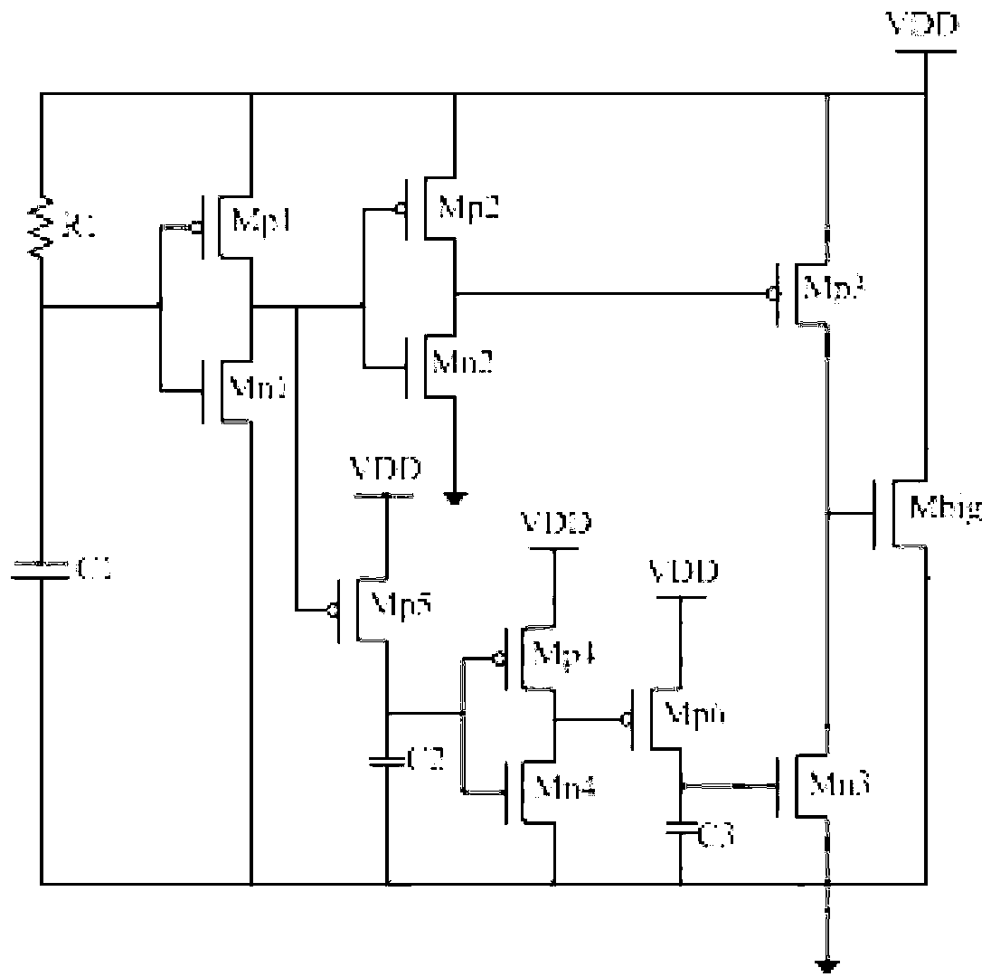
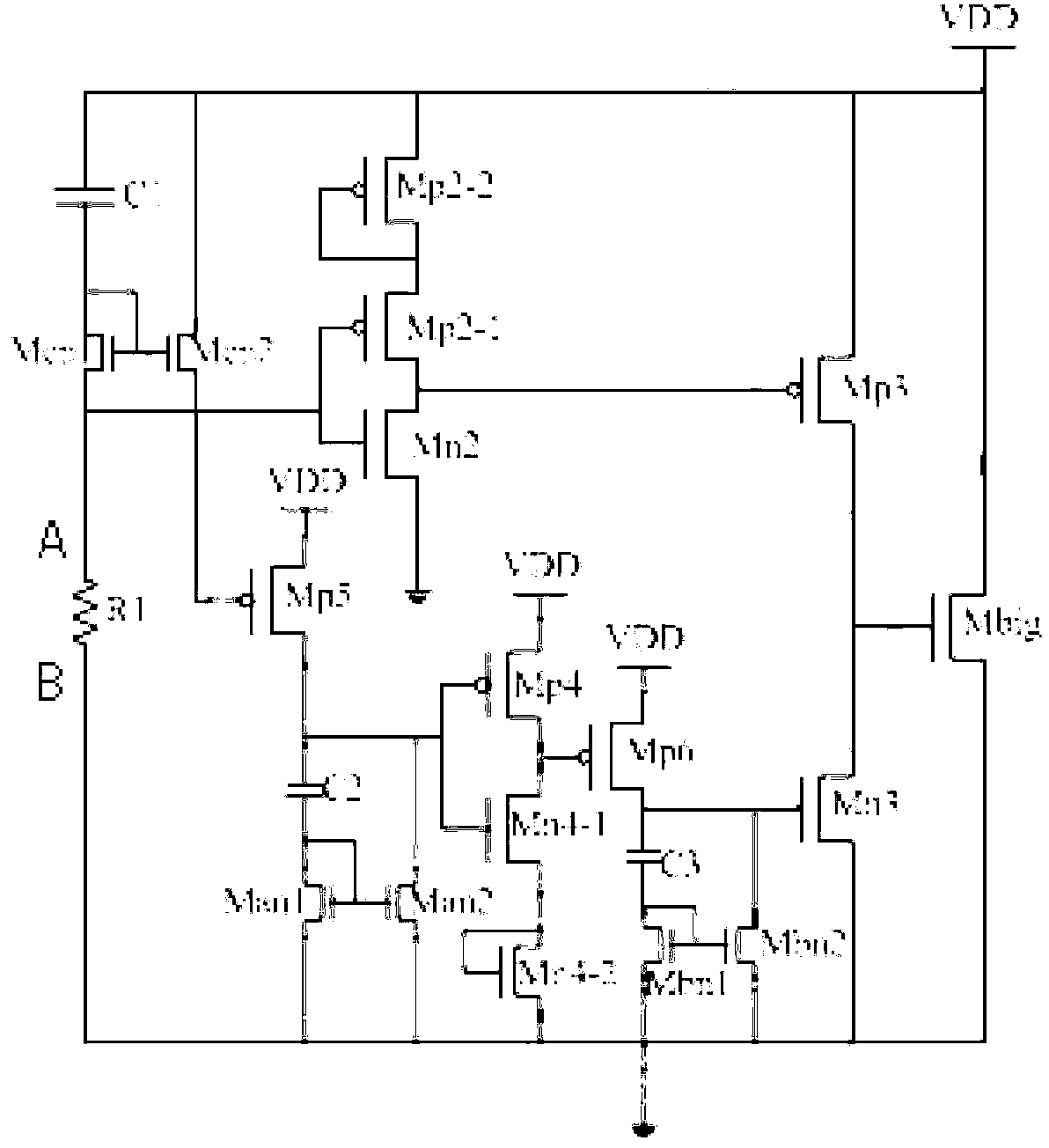
[0024] figure 2 It is a structural schematic diagram of an anti-false trigger type power supply clamp ESD protection circuit according to an embodiment of the present invention. The circuit includes: an ESD impact detection component, a discharge transistor, an opening path of the discharge transistor, and an off path of the discharge transistor.

[0025]The ESD impact detection part is used to identify whether the impact added between the power line and the ground wire is an ESD impact, if it is an ESD impact, a corresponding signal is sent to open the discharge transistor, and if it is powered on normally, the discharge transistor is not opened Transistor; the discharge transistor is used to provide a low-resistance discharge path for the electrostatic charge brought by the impact when the ESD impact comes; the discharge transistor opens the path f...


PUM


Abstract

The invention discloses an anti-false-triggering power supply clamp ESD (Electro-Static Discharge) protection circuit, which comprises an ESD impact detection part, a bleeding transistor, a bleeding transistor turning-on circuit and a bleeding transistor turning-off circuit. The anti-false-triggering power supply clamp ESD protection circuit has the advantages that the static charge bleeding capacity is very strong during ESD impact under the situation of small layout area, the leakage current is very small during normal electrification and the false triggering immunity is very strong during rapid electrification.

Description

technical field [0001] The invention relates to the field of integrated circuit chip electrostatic discharge (Electronic Static Discharge, ESD) protection technology, in particular to an anti-false trigger type power clamp ESD protection circuit. Background technique [0002] The electrostatic protection design of integrated circuit chips is one of the necessary conditions to ensure the reliable operation of chips. Electrostatic shock is ubiquitous in life. With the continuous advancement of integrated circuit technology, the size of the devices that make up the circuit is getting smaller and smaller. Electrostatic shock itself has the characteristics of short time and very large instantaneous current. When the device size is small Under normal circumstances, the electrostatic shock will form a huge equivalent electric field inside the device, which will directly break down the device, causing the device to suffer irreversible physical damage and be paralyzed. [0003] The ...

Claims


Application Information

Patent Timeline
Patent Type & Authority Applications(China)
IPC IPC(8): H02H9/00
CPCH02H9/00H02H9/046H02H9/045
Inventor 王源陆光易曹健刘琦贾嵩张兴
Owner PEKING UNIV
Why Eureka
Try Eureka