Heterojunction solar battery with electroplate electrodes and preparation method
A solar cell and heterojunction technology, applied in circuits, photovoltaic power generation, electrical components, etc., can solve the problems of metal electrode offset, high wire resistance, expensive metal silver, etc., to improve the conductivity of grid lines, improve battery performance, the effect of reducing shading loss
- Summary
- Abstract
- Description
- Claims
- Application Information
AI Technical Summary
Problems solved by technology
Method used
Image

Examples
Embodiment 1
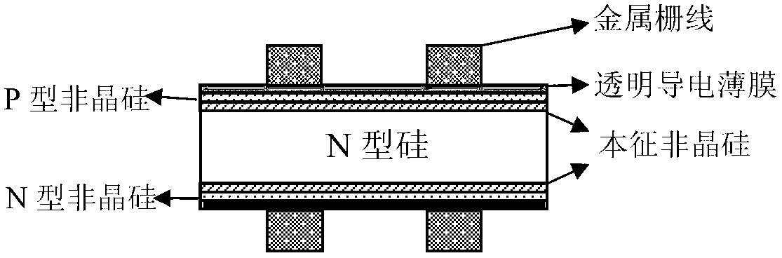
[0098] Example 1. Please see attached Figure 4
[0099] (a) Form a transparent conductive thin film layer on the base of the HIT battery, the base includes preparing a HIT battery on an n-type or p-type substrate, and depositing a transparent conductive thin film transparent to point thin film includes one or more The combination can be deposited by PECVD, PVD, RPD, etc., with a thickness between 1nm and 1um.
[0100] The process steps of the transparent conductive thin film layer are:
[0101] a) Removal of damage and surface texturing of the crystalline silicon substrate;
[0102] b) Depositing an intrinsic amorphous silicon layer (i-type a-Si), about 0-50nm;
[0103] c) Depositing an n-type amorphous silicon layer (n-type a-Si), about 1-50nm;
[0104] d) Depositing an intrinsic amorphous silicon layer (i-type a-Si), about 0-50nm;
[0105] e) Depositing a p-type amorphous silicon layer (p-type a-Si), about 1-50nm;
[0106] f) Depositing a transparent conductive film o...
Embodiment 2
[0114] Example 2 (see Figure 5 )
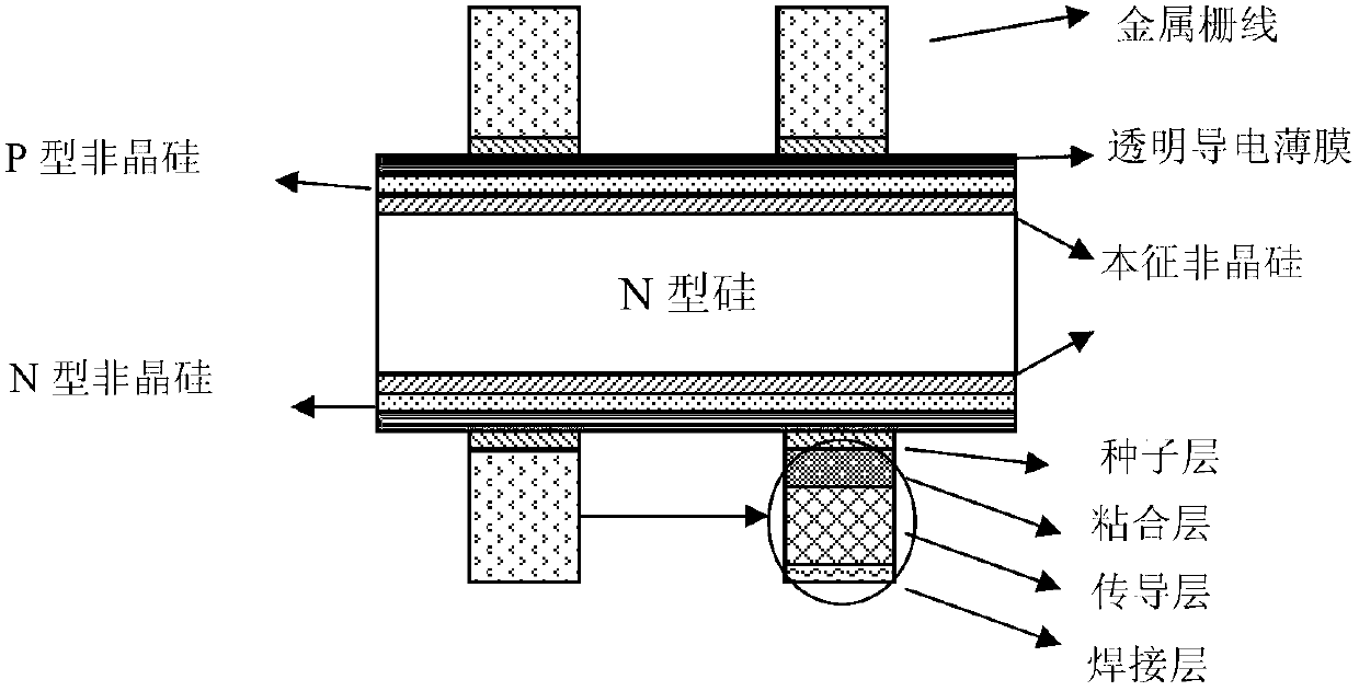
[0115] Similar to technical route 1, this method can also be used for double-sided electroplating of heterojunction solar cells. The specific process is as follows Figure 5 As shown, it is a derivative of technical route 1, which is also the technical protection category of the present invention.
[0116] Steps (a)-(c) and steps (e) and (g) are similar to embodiment 1 and step (d) is:
[0117] (d) Double-sided electroplating to form electrodes. One of Ni, Cu, Ag, Sn, Al, Cr, Au, etc., or a combined stacking form of several types is electroplated on the opening of the mask and on the metal seed layer by electroplating. The electroplating technology includes electrodeposition, light-induced deposition or chemical deposition, etc. Since the mask is insulating, the electroplated metal is deposited on both sides only at the opening of the mask and on the metal seed layer, thereby forming a double-sided metal gate line pattern. Figure 5 A s...
Embodiment 3
[0118] Example 3. See Image 6
[0119] (a) Forming a transparent conductive thin film layer on the HIT battery substrate, the substrate includes preparing a HIT battery on an n-type or p-type substrate, and depositing a transparent conductive thin film on it, the transparent conductive thin film includes those mentioned in the rights One or a combination of materials (but not limited to) can be deposited by PECVD, PVD, RPD, etc., with a thickness between 1nm and 1um.
[0120] The formation process of the transparent conductive thin film layer is the same as that of Embodiment 1.
[0121] (b) A mask is patterned. The mask can cover the resist on the seed layer by printing, spin coating, spraying, roller hot pressing, pulling, dipping, PECVD, etc. The mask materials include ink, polymer, dry film, photoresist, SiO 2 、SiN x One or a combination of several of them, using selective chemical etching, photolithography, plasma etching, laser etching, etc. to form the mask pattern...
PUM
| Property | Measurement | Unit |
|---|---|---|
| Thickness | aaaaa | aaaaa |
| Thickness | aaaaa | aaaaa |
| Thickness | aaaaa | aaaaa |
Abstract
Description
Claims
Application Information
 - R&D Engineer
- R&D Manager
- IP Professional
- Industry Leading Data Capabilities
- Powerful AI technology
- Patent DNA Extraction
Browse by: Latest US Patents, China's latest patents, Technical Efficacy Thesaurus, Application Domain, Technology Topic.
© 2024 PatSnap. All rights reserved.Legal|Privacy policy|Modern Slavery Act Transparency Statement|Sitemap