Array substrate and manufacturing method thereof and display device

An array substrate, substrate technology, applied in the field of array substrate and its manufacturing method and display device, can solve the problem of high cost, achieve the effect of increasing manufacturing cost, ensuring aperture ratio, and realizing narrow frame technology

Active Publication Date: 2013-05-22
BOE TECH GRP CO LTD +1
View PDF5 Cites 9 Cited by
  • Summary
  • Abstract
  • Description
  • Claims
  • Application Information

AI Technical Summary

Problems solved by technology

In this way, in order to ensure that only one mask is used in the active layer process, it is necessary to consider using a half tone mask or a gray tone mask. However, the cost of this mask process is very high.

Method used


Image

  • Array substrate and manufacturing method thereof and display device
  • Array substrate and manufacturing method thereof and display device
  • Array substrate and manufacturing method thereof and display device

Examples


Embodiment Construction

[0032] The following will clearly and completely describe the technical solutions in the embodiments of the present invention with reference to the accompanying drawings in the embodiments of the present invention. Obviously, the described embodiments are only some, not all, embodiments of the present invention. Based on the embodiments of the present invention, all other embodiments obtained by persons of ordinary skill in the art without making creative efforts belong to the protection scope of the present invention.

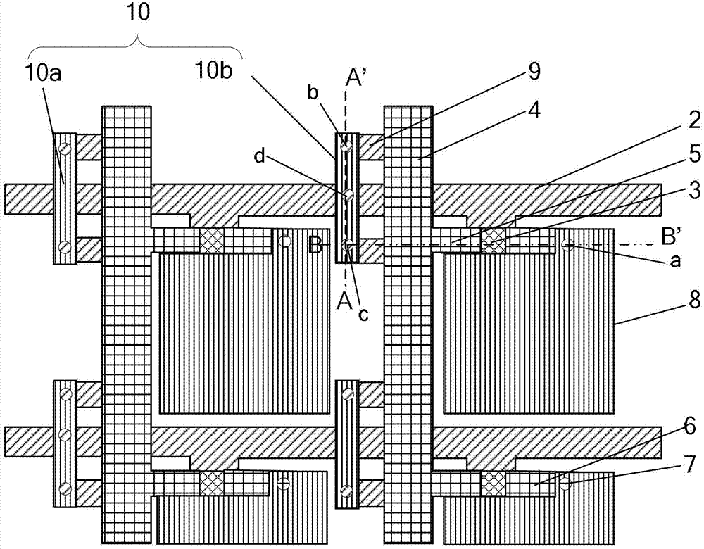
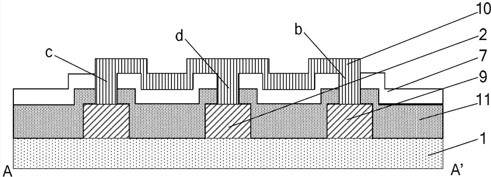
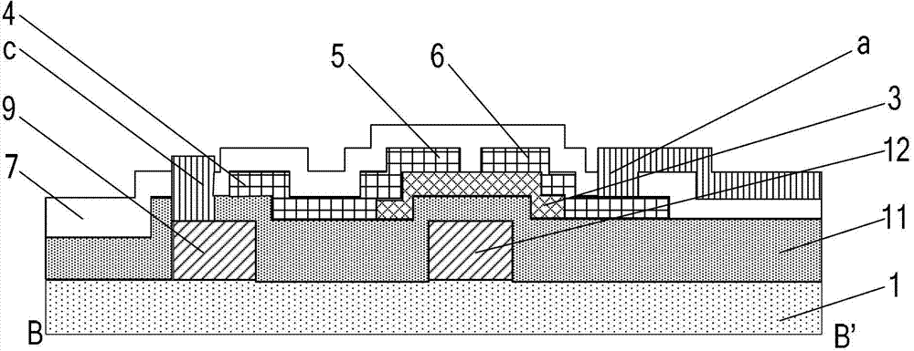
[0033] An embodiment of the present invention provides an array substrate, referring to figure 1 , 2 and 3, including:

[0034] The substrate 1; the gate 12 on the substrate, the gate line 2 and the first gate line 9 between the gate lines 2; the gate insulating layer 11 covering the gate 12, the gate line 2 and the first gate line 9 ; Active layer 3, source 5, drain 6 and data 4 lines above the gate insulating layer 11; Passivation layer 7 covering active l...


PUM


Abstract

An embodiment of the invention provides an array substrate and a manufacturing method thereof and a display device and relates to the technical field of display. The narrow Bezel technology is realized on the basis that aperture ratio is guaranteed while manufacturing cost is not increased. The array substrate comprises a substrate, grids positioned on the substrate, grid lines, first grid line leads among the grid lines, a grid insulating layer, an active layer, sources, drains, data lines and a passivation layer, the grid insulating layer is covered the grids, grid lines and the first grid line leads, the active layer, the sources, the drains and the data lines are positioned above the grid insulating layer and covered by the passivation layer, the grid lines partition the first grid line leads crossed with the grid lines, each first grid line lead comprises a signal transmission area and connecting areas positioned at two ends of the signal transmission area, the signal transmission areas are parallel to positioned below the data lines, and the connecting areas are positioned on one sides of the data lines. The array substrate and the manufacturing method thereof and the display device are applied to display manufacturing.

Description

technical field [0001] The present invention relates to the field of display technology, in particular to an array substrate, a manufacturing method thereof, and a display device. Background technique [0002] In the prior art, in order to realize a narrow frame display panel, the gate fan-out in active area (GIA for short) is divided into two parts. Part of the synchronization process with the gate line layer is completed, and the other part is completed with the data line layer synchronization process. The arrangement of the GIA lines is completed without increasing the process steps, and most of the GIA lines are arranged directly under the data lines, ensuring a high aperture ratio. However, in order not to increase the process steps, the GIA via hole needs to be completed on the active layer synchronously with the active layer process. In the active layer etching of the normal process, only the active layer needs to be etched, and the GI insulating layer needs to be r...

Claims


Application Information

Patent Timeline
Patent Type & Authority Applications(China)
IPC IPC(8): H01L27/12H01L21/77G09F9/33
Inventor 王本莲栗晓代磊韩静杨永菊蔡科
Owner BOE TECH GRP CO LTD
Why Eureka
Try Eureka