

A method for detecting whether a wafer is abnormal
A wafer, abnormal technology, applied in the field of detecting whether the wafer is abnormal, can solve the problem of abnormal wafer entry and loss, etc.
- Summary
- Abstract
- Description
- Claims
- Application Information
AI Technical Summary
Problems solved by technology
Method used
Image

Examples
Embodiment Construction
[0026] The following will clearly and completely describe the technical solutions in the embodiments of the present invention with reference to the accompanying drawings in the embodiments of the present invention. Obviously, the described embodiments are only some, not all, embodiments of the present invention. Based on the embodiments of the present invention, all other embodiments obtained by persons of ordinary skill in the art without making creative efforts belong to the protection scope of the present invention.
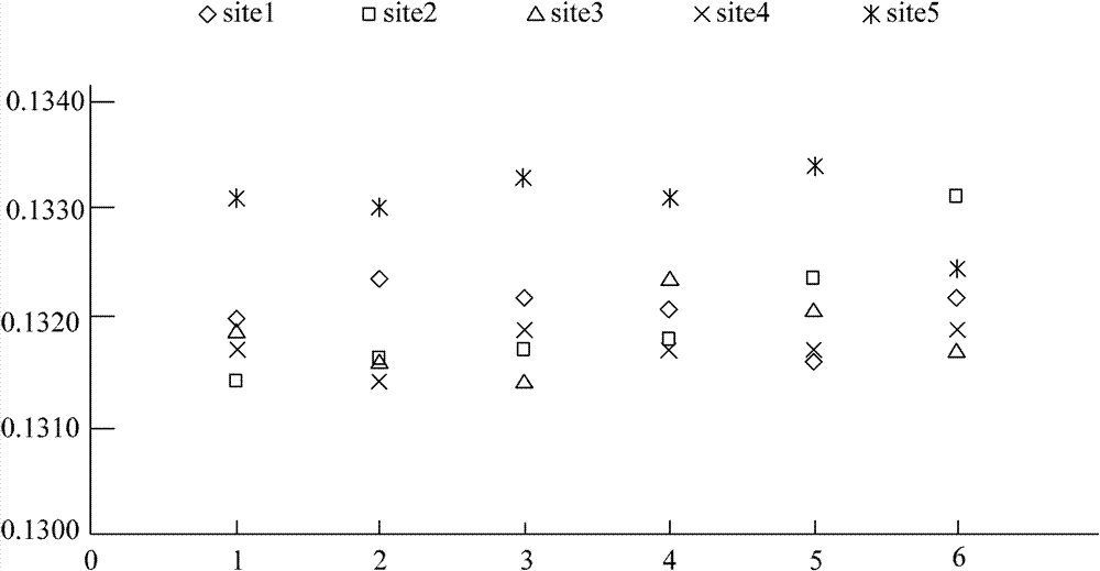
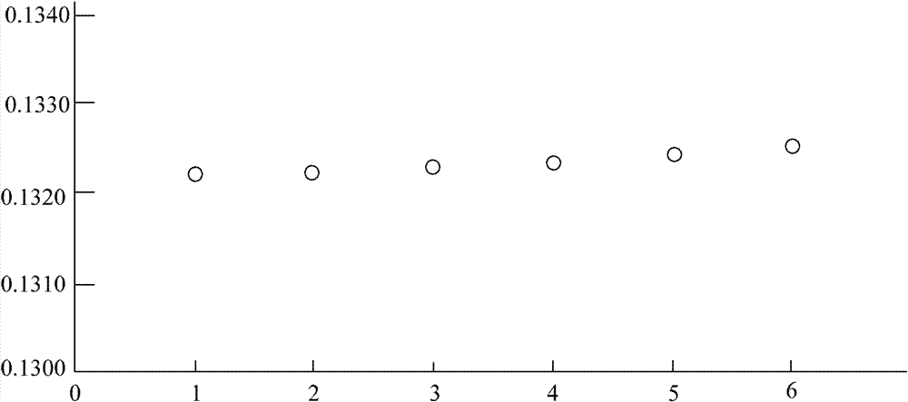
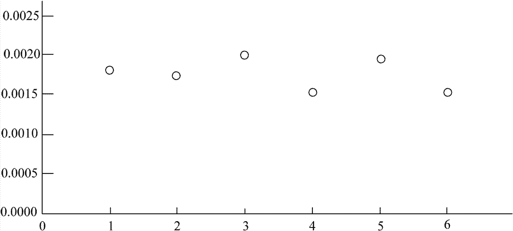
[0027] According to the background technology section and combined with Figure 1 ~ Figure 3 It can be seen that when detecting whether the wafer is abnormal, if the collected raw data on the wafer is processed by the mean value method or the range method, sometimes the abnormality of the wafer cannot be detected. Therefore, the present invention finds a new way and adopts a new method to process the original data, so as to detect the abnormal phenomenon of th...
PUM
 Abstract
Description
Claims
Application Information