
Organic light-emitting display device and method of manufacturing the same

一种发光显示、有机的技术,应用在半导体/固态器件制造、电气元件、电固体器件等方向,能够解决投入成本增加、需要设备大的空间、不能够布置设备等问题

Active Publication Date: 2013-06-19
SAMSUNG DISPLAY CO LTD
View PDF1 Cites 4 Cited by
  • Summary
  • Abstract
  • Description
  • Claims
  • Application Information

AI Technical Summary

Problems solved by technology

In the case of using a deposition method, the solvent used for the intermediate layer, for example, the solvent used for the solution of HTL, dissolves EML during the deposition process, deteriorating the interface characteristics
In addition, by utilizing both the nozzle printing method and the deposition method, input costs may increase, a large space for equipment may be required, and it may be difficult or impossible to arrange in-line based equipment

Method used


Image

  • Organic light-emitting display device and method of manufacturing the same
  • Organic light-emitting display device and method of manufacturing the same
  • Organic light-emitting display device and method of manufacturing the same

Examples


Embodiment Construction

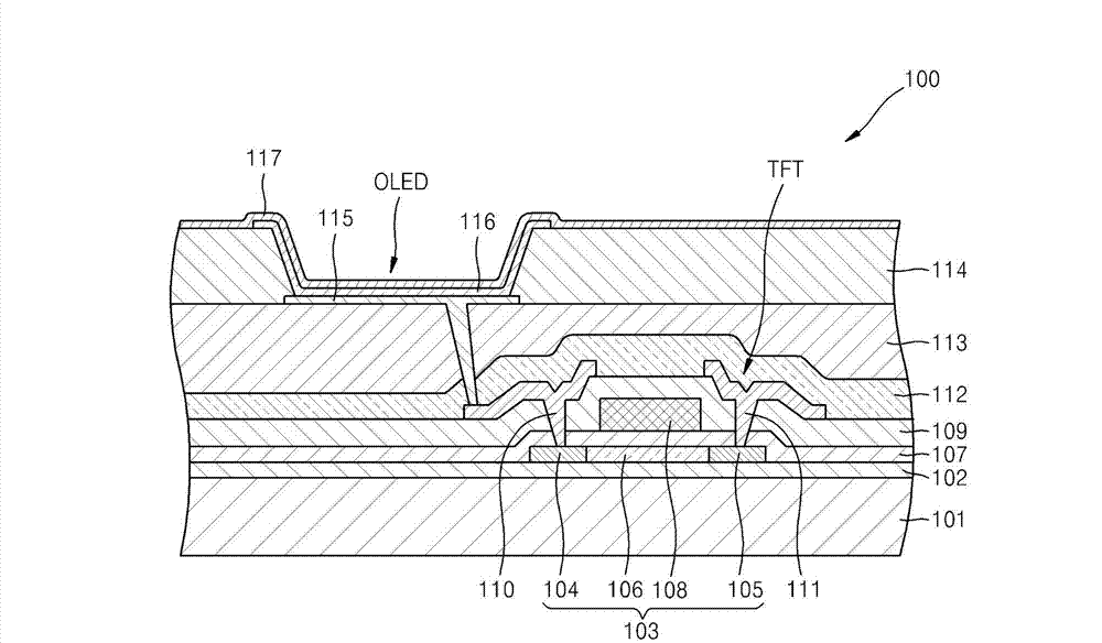
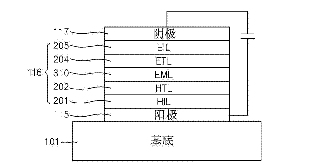
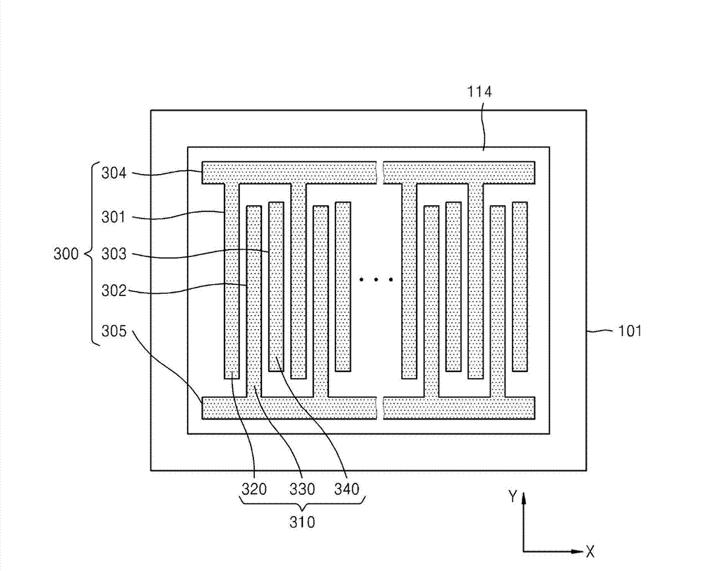
[0040] The present invention will now be described more fully with reference to the accompanying drawings, in which exemplary embodiments of the invention are shown. However, this invention may be embodied in many different forms and should not be construed as limited to the embodiments set forth herein. Therefore, the present invention may include all modifications, equivalents, or substitutes included within the concept and technical scope related to the present invention. In describing the embodiments of the present invention, when certain detailed descriptions of the prior art are considered to unnecessarily obscure the essence of the present invention, their detailed descriptions may be omitted.

[0041] Although terms such as 'first', 'second', etc. may be used to describe various components, these components should not be limited by the above terms. The above terms are often used to distinguish one component from another.

[0042] The terms used in this specification ...


PUM


Abstract

In an organic light-emitting display device and a method of manufacturing the organic light-emitting display device, the method includes forming thin film transistors (TFTs) on a substrate; and forming organic light emitting diodes (OLEDs), each of the OLEDs including a first electrode having a portion exposed by a pixel defining layer (PDL) on the TFTs, an organic layer on the exposed portion of the first electrode and including an emission layer (EML) configured to emit light having a respective one of a plurality of colors, and a second electrode on the organic layer. The EML is formed in each of a sub-pixel region with one color and other sub-pixel regions with other colors that are formed by forming openings in the PDL. A solution supply unit for sub-pixel region that communicates with the sub-pixel region with one color is formed in the sub-pixel region with one color.

Description

[0001] This application claims priority and benefit from Korean Patent Application No. 10-2011-0137408 filed in the Korean Intellectual Property Office on December 19, 2011, the disclosure of which is hereby incorporated by reference in its entirety. technical field [0002] The present invention relates to an organic light emitting display device and a method for manufacturing the organic light emitting display device. Background technique [0003] In general, organic light-emitting display devices can be applied to mobile devices (such as digital cameras, video cameras, camcorders, portable information terminals, smart phones, ultra-thin notebooks, desktop personal computers, and flexible display devices) or electronic / electrical devices (such as ultra-thin TVs) machine) display device. [0004] An organic light emitting display device has a stack structure in which an emission layer (EML) is interposed between an anode and a cathode. However, it is difficult to obtain hi...

Claims


Application Information

Patent Timeline
Patent Type & Authority Applications(China)
IPC IPC(8): H01L21/77H01L51/56H01L27/32H01L51/50
CPCH01L27/1292H10K59/35H10K71/13H10K59/12H10K71/40H10K59/1201H10K71/00H10K50/00
Inventor 赵晟焕
Owner SAMSUNG DISPLAY CO LTD
Features
  • Generate Ideas
  • Intellectual Property
  • Life Sciences
  • Materials
  • Tech Scout
  • Unparalleled Data Quality
  • Higher Quality Content
  • 60% Fewer Hallucinations
Learn More