Organic light emitting device and method for manufacturing the same

A technology of organic light-emitting devices and light-emitting layers, which is applied in the fields of organic semiconductor devices, semiconductor/solid-state device manufacturing, and electric solid-state devices, and can solve problems such as difficult multiple layers, damage, and inapplicability

Active Publication Date: 2013-07-03
LG DISPLAY CO LTD
View PDF3 Cites 9 Cited by
  • Summary
  • Abstract
  • Description
  • Claims
  • Application Information

AI Technical Summary

Problems solved by technology

However, these structures have a problem that the driving voltage increases when the color purity increases
Hybrid OLEDs with improved color purity and reduced driving voltage have not yet been developed
[0013] In addition, solution processing needs to be applied to hybrid devices, but there are layers that are not suitable for solution processing due to inherent limitations of materials, and thus, it is difficult to stabilize due to damage to the surface of layers formed when solution processing and vacuum deposition are used in combination. Apply solution processing to multiple layers efficiently

Method used


Image

  • Organic light emitting device and method for manufacturing the same
  • Organic light emitting device and method for manufacturing the same
  • Organic light emitting device and method for manufacturing the same

Examples


Embodiment Construction

[0037] Specific embodiments of the invention will now be described in detail, examples of preferred embodiments of the invention are illustrated in the accompanying drawings. Wherever possible, the same reference numbers will be used throughout the drawings to refer to the same or like components.

[0038] Hereinafter, an organic light emitting device and a method of manufacturing the same according to the present invention will be described in detail with reference to the accompanying drawings.

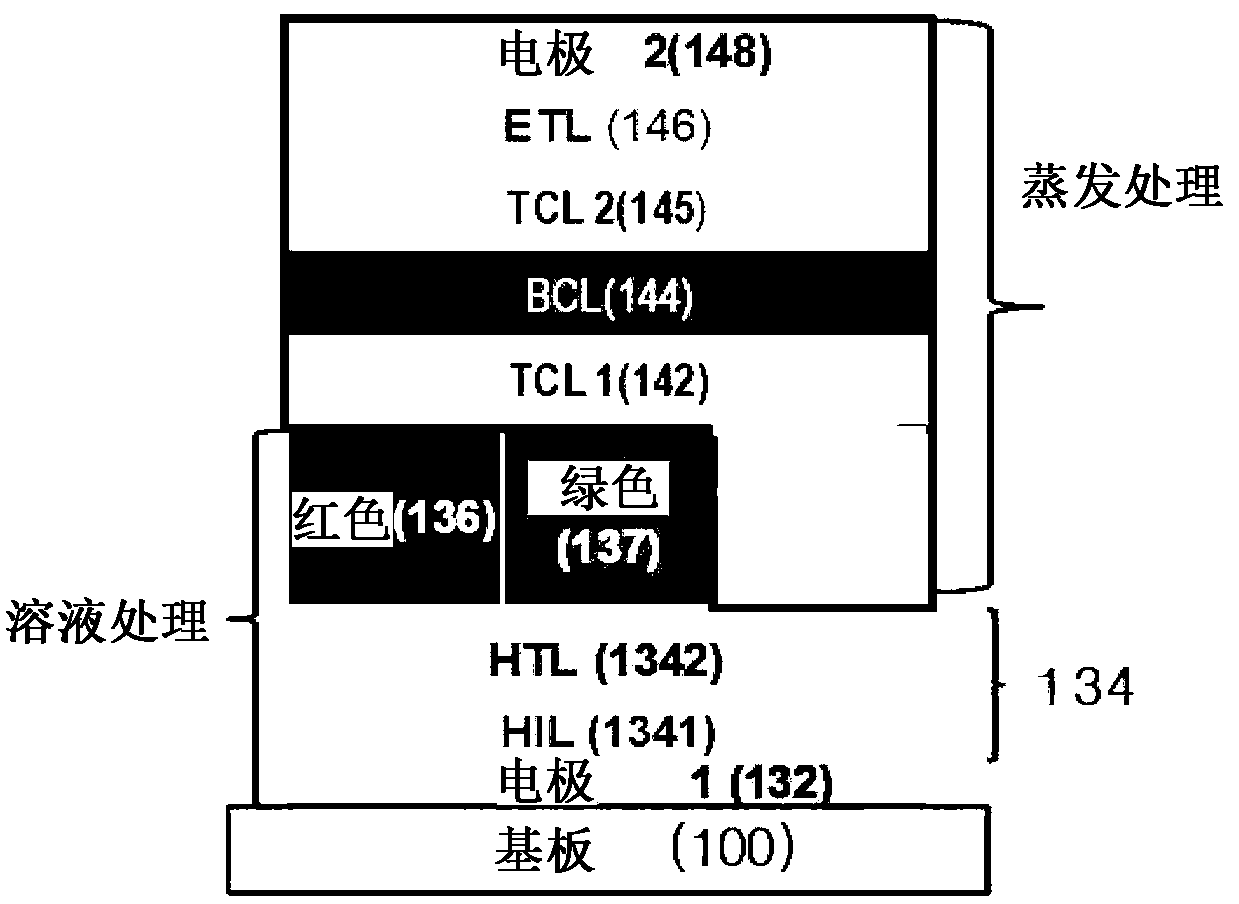
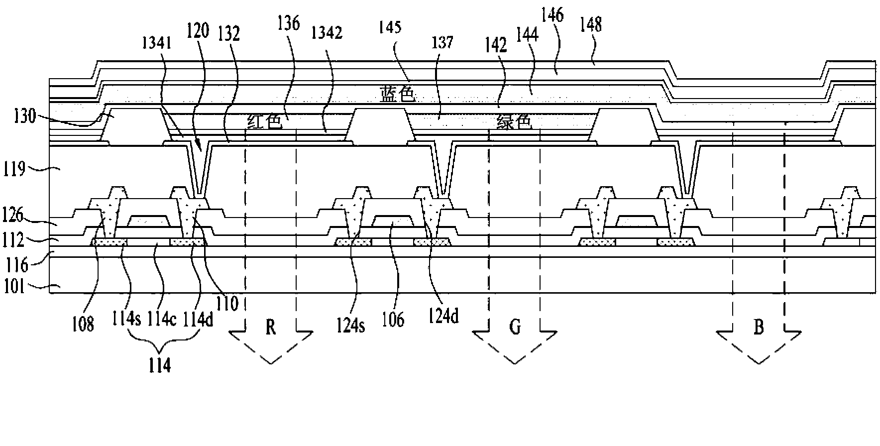
[0039] figure 1 is a sectional view illustrating an organic light emitting device according to the present invention.

[0040] Such as figure 1As shown, the organic light emitting device includes a TFT substrate 100 divided into and defined by first to third pixels, a first electrode 132 arranged on the TFT substrate, facing the first electrode 132 and connected to the first electrode 132. A second electrode 148 separated by an electrode 132, a first light emitting layer 136 arran...


PUM


Abstract

The present disclosure relates to an organic light emitting device, efficiency of which is improved by changing a layer structure, and a method for manufacturing the same. The organic light emitting device includes a substrate divided into and defined by first to third pixels, a first electrode disposed on the substrate and a second electrode facing the first electrode, a first light emitting layer and a second light emitting layer disposed in the first pixel and in the second pixel, respectively, between the first electrode and the second electrode, a first triplet exciton confinement layer, a third light emitting layer and a second triplet exciton confinement layer disposed over the first to third pixels in this order, on the first light emitting layer and the second light emitting layer, and a first common layer disposed between the first light emitting layer and the second light emitting layer, and the first electrode, and a second common layer disposed between the second triplet exciton confinement layer and the second electrode.

Description

technical field [0001] The present invention relates to an organic light-emitting device, and more particularly to an organic light-emitting device whose efficiency is improved by changing a layer structure and a manufacturing method thereof. Background technique [0002] As the core technology of the screen information communication era, image display devices that display various information on the screen are being developed toward thinner, lighter, portable, and higher-function trends. For this reason, as a cathode ray tube (CRT) Flat panel display devices that have problems of large weight and volume, organic light emitting displays that display images while controlling the amount of light from a light emitting layer attract much attention. [0003] Organic light-emitting displays emit light simultaneously using a thin light-emitting layer disposed between electrodes, thus advantageously realizing a paper-like film. Such an organic light emitting display is classified in...

Claims


Application Information

Patent Timeline
Patent Type & Authority Applications(China)
IPC IPC(8): H01L51/52H01L51/56
CPCH10K71/16H10K71/12H10K50/11H10K2101/40H10K2102/103H10K71/00H10K59/805H10K50/805H10K59/1201
Inventor 南栋熙李煐九金禧镇李学旻
Owner LG DISPLAY CO LTD
Why Eureka
Try Eureka