Substrate align marks and manufacturing method thereof and substrate
An alignment mark and production method technology, which is applied in the photoengraving process of the pattern surface, semiconductor/solid-state device manufacturing, semiconductor/solid-state device parts and other directions, can solve the problems of uneven coating, inability to identify alignment marks, etc. The effect of reducing the defective rate and improving the recognition success rate
- Summary
- Abstract
- Description
- Claims
- Application Information
AI Technical Summary
Problems solved by technology
Method used
Image
Examples
Embodiment 1
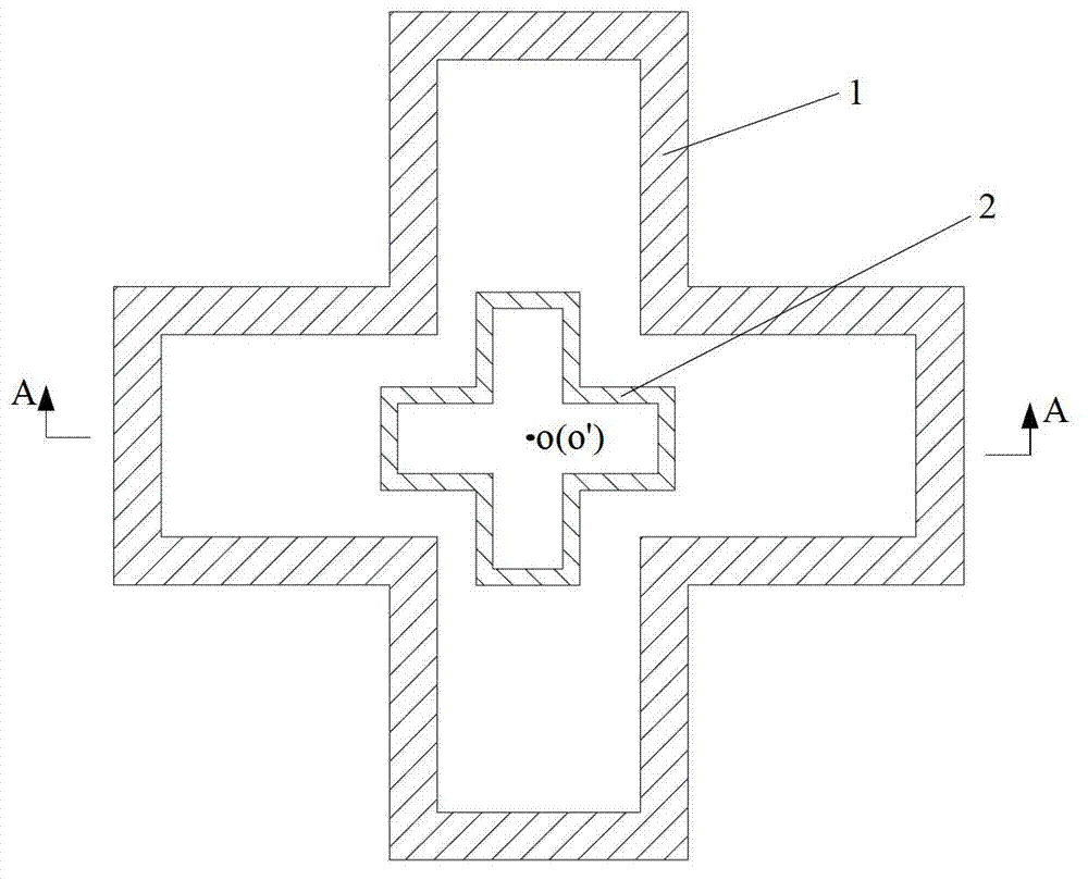
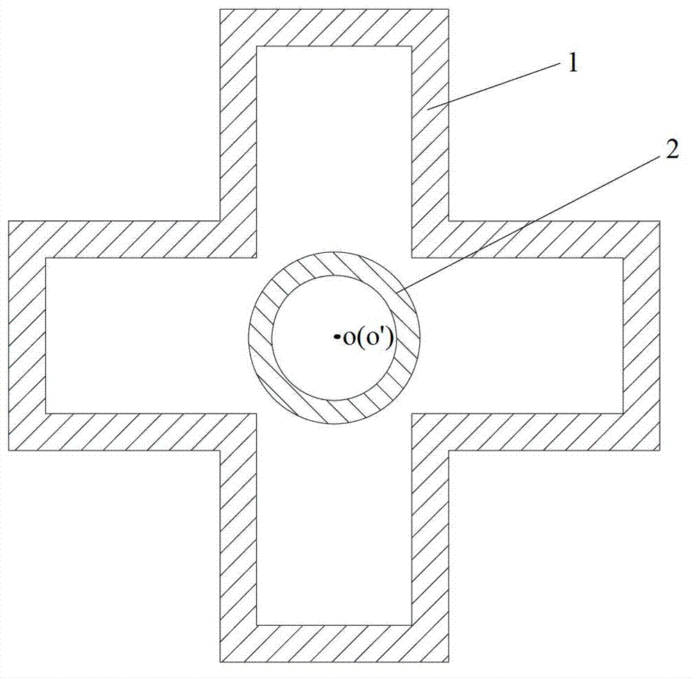
[0037] In order to improve the recognition success rate of alignment marks in the substrate manufacturing process, this embodiment provides a method for manufacturing alignment marks on a substrate, which includes the step of forming a first alignment mark pattern and the step of forming a second alignment mark pattern . Wherein, the first alignment mark pattern and the second alignment mark pattern are located on different layer structures of the substrate (here, different layer structures refer to patterns formed by different layers of thin films on the substrate, and correspondingly, the same layer structure refers to patterns on the substrate. pattern formed by the same layer of film), and the centers coincide, that is, the centers of the first alignment mark pattern and the second alignment mark pattern correspond up and down, and are located on a straight line, so that when the alignment is performed through the two alignment marks respectively, Can maintain alignment co...
Embodiment 2
[0045] Correspondingly, this embodiment also provides a substrate alignment mark, combined with Figure 1-Figure 5 As shown, the substrate alignment mark includes different layer structures on the substrate (different layer structures here refer to patterns formed by different layers of thin films on the substrate, and correspondingly, the same layer structure refers to patterns formed by the same layer of thin films on the substrate) The first alignment mark pattern 1 and the second alignment mark pattern 2, wherein the center o of the first alignment mark pattern 1 and the center o' of the second alignment mark pattern 2 coincide, that is, the first alignment mark The centers o and o' of the pattern 1 and the second alignment mark pattern 2 correspond up and down, and are located on a straight line, so that the consistency of alignment can be maintained when two alignment marks are used for alignment respectively. Moreover, there is no overlapping portion between the first a...
Embodiment 3
[0049] This embodiment provides a substrate with an alignment mark on it, and the alignment mark adopts the substrate alignment mark in Embodiment 2. Since the success rate of alignment mark identification is improved, the production process of the substrate is greatly reduced. In the defect rate due to the inability to recognize the registration mark.
[0050] For the array substrate of TFT-LCD, thin film transistors are formed on it, in the actual application process, combined with figure 1 As shown, the first alignment mark pattern 1 can be designed to be made of the same metal layer as the gate electrode of the thin film transistor, and the second alignment mark pattern 2 is made of the same metal layer as the source and drain electrodes of the thin film transistor.
[0051] It can be seen from the above embodiments that the substrate alignment mark and its manufacturing method provided by the present invention, by making two alignment mark patterns on different layer stru...
PUM
 Abstract
Description
Claims
Application Information
 - R&D
- Intellectual Property
- Life Sciences
- Materials
- Tech Scout
- Unparalleled Data Quality
- Higher Quality Content
- 60% Fewer Hallucinations
Browse by: Latest US Patents, China's latest patents, Technical Efficacy Thesaurus, Application Domain, Technology Topic, Popular Technical Reports.
© 2025 PatSnap. All rights reserved.Legal|Privacy policy|Modern Slavery Act Transparency Statement|Sitemap|About US| Contact US: help@patsnap.com


