Shifting register unit, gate driving circuit and display device

A shift register, gate connection technology, applied in the field of gate drive circuits, display devices, and shift register units, can solve the problems of complex structure, difficult to use number of transistors, etc., to simplify the structure, reduce the number of use, and reduce the number of Effect

Active Publication Date: 2013-07-17
BOE TECH GRP CO LTD +1
7 Cites 70 Cited by

AI-Extracted Technical Summary

Problems solved by technology

With the continuous development of display devices, people's demand for narrow bezel display devices is also increasing. The key to narrow bezel display devices is how to further reduce the number of transistors used in the GOA circuit. ...

Method used

[0083] With such a structured shift register unit, bidirectional scanning of the gate drive circuit can be realized by changing the level of the control signal. Specifically, the driving method and wor...

Abstract

The embodiment of the invention provides a shifting register unit, a gate driving circuit and a display device, and relates to the technical field of display. The shifting register unit comprises an input module, a first output module and a second output module. Compared with the prior art, the invention has the advantages that the structure of the shifting register unit can be effectively simplified; and the using quantity of transistors is further decreased. The embodiment of the invention is used for realizing scanning driving.

Application Domain

Static indicating devicesDigital storage

Technology Topic

Shift registerDisplay device +3

Image

  • Shifting register unit, gate driving circuit and display device
  • Shifting register unit, gate driving circuit and display device
  • Shifting register unit, gate driving circuit and display device

Examples

  • Experimental program(1)

Example Embodiment

[0021] The technical solutions in the embodiments of the present invention will be clearly and completely described below in conjunction with the accompanying drawings in the embodiments of the present invention. Obviously, the described embodiments are only a part of the embodiments of the present invention, rather than all the embodiments. Based on the embodiments of the present invention, all other embodiments obtained by a person of ordinary skill in the art fall within the protection scope of the present invention.
[0022] The transistors used in all the embodiments of the present invention can be thin film transistors or field effect transistors or other devices with the same characteristics. Since the source and drain of the transistors used here are symmetrical, there is no difference between the source and drain. of. In the embodiment of the present invention, in order to distinguish the two poles of the transistor except the gate, one of them is called the first pole, and the other pole is called the second pole. In addition, transistors can be divided into N-type and P-type according to their characteristics. In the embodiment of the present invention, each stage of shift register unit may include multiple N-type transistors and multiple P-type transistors at the same time. The first pole of the transistor can be the source of the transistor, and the second pole of the transistor can be the drain of the transistor.
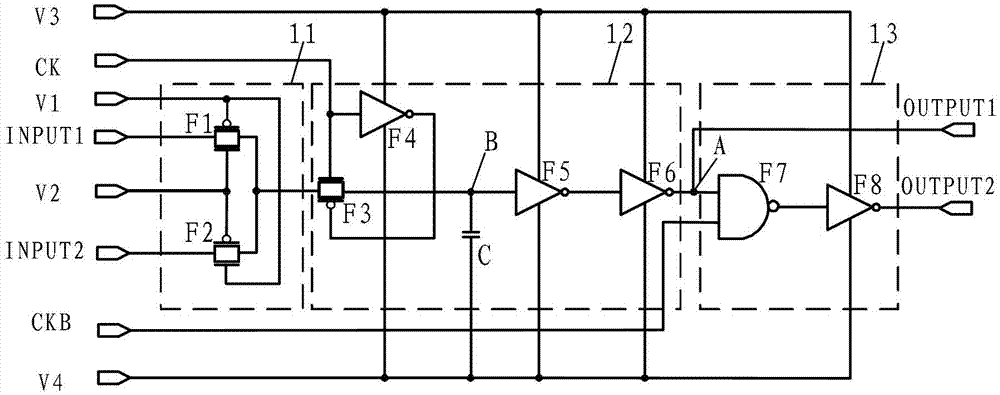
[0023] The shift register unit provided by the embodiment of the present invention, such as figure 1 As shown, it includes: an input module 11, a first output module 12, and a second output module 13.
[0024] Among them, the input module 11 is connected to the first signal input terminal INPUT1, the second signal input terminal INPUT2, the first voltage terminal V1, the second voltage terminal V2 and the first output module 12, and is used for inputting according to the first signal input terminal INPUT1 The signal, the signal input from the second signal input terminal INPUT2, the voltage input from the first voltage terminal V1, and the voltage input from the second voltage terminal V2 control the scanning direction of the shift register unit.
[0025] The first output module 12 is connected to the first clock signal terminal CK, the first node A, and the first signal output terminal OUTPUT1, and is used to control the first clock signal according to the signal input by the input module 11 and the first clock signal input from the first clock signal terminal CK A signal output terminal OUTPUT1 outputs the potential of the signal, and the first node A is the connection point between the first output module 12 and the second output module 13.
[0026] The second output module 13 is connected to the first node A, the second clock signal terminal CKB, and the second signal output terminal OUTPUT2, and is used for controlling according to the signal of the first node A and the second clock signal input from the second clock signal terminal CKB The second signal output terminal OUTPUT2 outputs the potential of the signal.
[0027] The shift register unit provided by the embodiment of the present invention can effectively reduce the number of functional modules in the shift register unit and simplify the structure of the shift register unit, thereby further reducing the number of transistors used, thereby ensuring stable operation of the circuit while achieving The narrow bezel design of the display device is improved.
[0028] Further, as figure 2 As shown, in the shift register provided in the embodiment of the present invention, the input module 11 may include:
[0029] The first transmission gate F1 is connected to the first signal input terminal INPUT1, the first voltage terminal V1 and the second voltage terminal V2, respectively, and the output terminal of the first transmission gate F1 is connected to the first output module 12.
[0030] The second transmission gate F2 is respectively connected to the second signal input terminal INPUT2, the first voltage terminal V1 and the second voltage terminal V2, and the output terminal of the second transmission gate F2 is connected to the first output module.
[0031] It should be noted that the shift register unit provided in the embodiment of the present invention may include multiple transmission gate circuits, and the transmission gate circuits may be used as analog switches for transmitting analog signals, and each transmission gate circuit may include a set of N-type transistors and P-type transistors arranged in parallel. Of course, the transmission gate circuit can also adopt other circuit structures or components with switching functions in the prior art, which is not limited in the present invention.
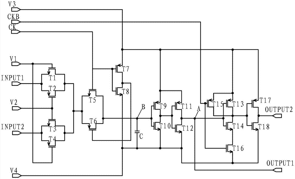
[0032] Specific, such as image 3 As shown, the first transmission gate F1 may include:
[0033] The first transistor T1, the first electrode of the first transistor T1 is connected to the first signal input terminal INPUT1, the gate of the first transistor T1 is connected to the first voltage terminal V1, and the second electrode of the first transistor T1 is connected to the first output Module 12.
[0034] The second transistor T2, the first electrode of the second transistor T2 is connected to the first signal input terminal INPUT1, the gate of the second transistor T2 is connected to the second voltage terminal V2, and the second electrode of the second transistor T2 is connected to the first output Module 12.
[0035] The second transmission gate F2 may include:
[0036] The third transistor T3, the first electrode of the third transistor T3 is connected to the second signal input terminal INPUT2, the gate of the third transistor T3 is connected to the second voltage terminal V2, and the second electrode of the third transistor T3 is connected to the first output Module 12.
[0037] A fourth transistor T4. The first electrode of the fourth transistor T4 is connected to the second signal input terminal INPUT2, the gate of the fourth transistor T4 is connected to the first voltage terminal V1, and the second electrode of the fourth transistor T4 is connected to the One output module 12.
[0038] The input module 11 adopts such a structure. When the signals output by the upper and lower shift register units are respectively used as the input signals of the first signal input terminal INPUT1 or the second signal control terminal INPUT2 of the shift register unit of this stage, the input module 11 can realize bidirectional scanning of the gate drive circuit. Specifically, the first signal input terminal INPUT1 may input the signal N-1OUT output by the first signal output terminal OUTPUT1 of the upper-level shift register unit, and the second signal input terminal INPUT2 may input the first signal output terminal OUTPUT1 of the lower-level shift register unit The output signal N+1 OUT.
[0039] In such image 3 In the shift register unit shown, the first transistor T1 and the third transistor T3 are N-type transistors, and the second transistor T2 and the fourth transistor T4 are P-type transistors. For the input module 11 with such a structure, when the first voltage terminal V1 inputs a high level VDD and the second voltage terminal V2 inputs a low level VSS, the high level output by the upper-level shift register unit can pass through the input module 11. The first output module 12 is precharged, and the high level output by the lower-level shift register unit can be reset to the first output module 12 through the input module 11, so as to realize the scanning drive of the gate driving circuit from top to bottom.
[0040] When the first voltage terminal V1 inputs low level VSS and the second voltage terminal V2 inputs high level VDD, the high level output by the lower-level shift register unit can precharge the first input module 12 through the input module 11, and the upper level The high level output by the shift register unit can reset the first input module 12 through the input module 11, so as to realize the bottom-up scan driving of the gate drive circuit.
[0041] Alternatively, the first signal input terminal INPUT1 may also input the signal N+1 OUT output by the first signal output terminal OUTPUT1 of the lower-level shift register unit, and the second signal input terminal INPUT2 may also input the first signal output of the upper-level shift register unit The signal N-1 OUT output from the terminal OUTPUT1. The bidirectional scanning of the gate driving circuit can also be realized by using the first voltage terminal V1 and the second voltage terminal V2 opposite to the foregoing.
[0042] It should be noted that the above is only an example of bidirectional scanning of the input module 11. It should be understood that when the first transistor T1 and the third transistor T3 are P-type transistors, and the second transistor T2 and the fourth transistor T4 are N-type transistors, the input voltage of the first voltage terminal V1 and the second voltage terminal V2 is changed. The bidirectional scanning of the gate drive circuit can also be realized.
[0043] Further, as figure 2 As shown, in the shift register provided by the embodiment of the present invention, the first output module 12 may include:
[0044] The third transmission gate F3 is respectively connected to the input module 11 and the first clock signal terminal CK. The output terminal of the third transmission gate F3 is connected to the second node B. The second node B is the output terminal of the third transmission gate F3 and the first A point between node A. It should be noted that in this embodiment, the second node B and the first node A may be the same.
[0045] A capacitor C, one end of the capacitor C is connected to the second node B, and the other end of the capacitor C is connected to the fourth voltage terminal V4.
[0046] The first inverter F4 is connected to the first clock signal terminal CK, the third voltage terminal V3, and the fourth voltage terminal V4, respectively. The output terminal of the first inverter F4 is connected to the control terminal of the third transmission gate F3.
[0047] It should be noted that the shift register unit provided by the embodiment of the present invention may include a plurality of inverter circuits, and the inverter circuit may perform 180° inversion processing on the phase of the input signal, each of which is reversed Each phaser circuit may include a pair of N-type transistors and P-type transistors arranged in series. Of course, the inverter circuit can also adopt other circuit structures or components with inverting functions in the prior art, which is not limited by the present invention.
[0048] The third voltage terminal V3 may be a high level VDD, and the fourth voltage terminal V4 may be a ground terminal or a low level VSS. The first output module 12 adopts such a circuit structure to control the potential of the output signal of the first signal output terminal OUTPUT1 according to the change of the input signal potential of the input module 11. The signal output from the first signal output terminal OUTPUT1 can be input to the upper or lower stage. The signal input terminal of the bit register unit is used as an open or reset signal to realize bidirectional scanning of the gate drive circuit.
[0049] In the actual application process, the first node A and the second node B may be different nodes. Since the potential of the second node B meets the timing of the signal output by the first signal output terminal OUTPUT1, the second node B can be connected to the first node B. A signal output terminal OUTPUT1 is connected. However, its disadvantage is that the driving capability at the second node B is relatively low, which makes it difficult to drive a large-scale circuit, which further affects the product quality of the display device.
[0050] In order to improve the driving capability of the signal output by the first signal output terminal OUTPUT1, such as figure 2 As shown, the first output module 12 may further include:
[0051] At least a pair of inverters connected in series is included between the first node A and the second node B.
[0052] Wherein, the first signal output terminal OUTPUT1 is connected to the first node A. Since the inverter has the effect of improving the driving capability, the structure of the series-paired inverter can be used to effectively improve the driving capability of the output signal of the first signal output terminal OUTPUT1 without changing the phase of the output signal. For example, in figure 2 In the shift register unit shown, there is a pair of inverters connected in series between the first node A and the second node B, which are the second inverter F5 and the third inverter F6, respectively.
[0053] Specific, such as image 3 As shown, the third transmission gate F3 may include:
[0054] A fifth transistor T5. The first pole of the fifth transistor T5 is connected to the input module 11, the gate of the fifth transistor T5 is connected to the first clock signal terminal CK, and the second pole of the fifth transistor T5 is connected to the second node B.
[0055] A sixth transistor T6, the first pole of the sixth transistor T6 is connected to the input module 11, and the second pole of the sixth transistor T6 is connected to the second node B.
[0056] The first inverter F4 may include:
[0057] A seventh transistor T7, the first electrode of the seventh transistor T7 is connected to the third voltage terminal V3, the gate of the seventh transistor T7 is connected to the first clock signal terminal CK, and the second electrode of the seventh transistor T7 is connected to the sixth transistor The gate of T6.
[0058] An eighth transistor T8. The first pole of the eighth transistor T8 is connected to the fourth voltage terminal V4, the gate of the eighth transistor T8 is connected to the first clock signal terminal CK, and the second pole of the eighth transistor T8 is connected to the sixth transistor T6. Gate.
[0059] There is a second inverter F5 and a third inverter F6 connected in series between the first node A and the second node B, and the second inverter F5 includes:
[0060] A ninth transistor T9. The first electrode of the ninth transistor T9 is connected to the third voltage terminal V3, the gate of the ninth transistor T9 is connected to the second node B, and the second electrode of the ninth transistor T9 is connected to the third inverter F6.
[0061] A tenth transistor T10, the first electrode of the tenth transistor T10 is connected to the fourth voltage terminal V4, the gate of the tenth transistor T10 is connected to the second node B, and the second electrode of the tenth transistor T10 is connected to the third inverter F6.
[0062] The third inverter F6 includes:
[0063] The eleventh transistor T11, the first pole of the eleventh transistor T11 is connected to the third voltage terminal V3, the gate of the eleventh transistor T11 is connected to the second inverter F5, and the second pole of the eleventh transistor T11 Connect the first node A.
[0064] The twelfth transistor T12, the first pole of the twelfth transistor T12 is connected to the fourth voltage terminal V4, the gate of the twelfth transistor T12 is connected to the second inverter F5, and the second pole of the twelfth transistor T12 Connect the first node A.
[0065] Specifically, the second pole of the ninth transistor T9 and the second pole of the tenth transistor T10 are respectively connected to the gate of the eleventh transistor T11 and the gate of the twelfth transistor T12, thereby realizing the second inverter F5 The output terminal is connected to the input terminal of the third inverter F6.
[0066] Of course, more pairs of inverters can be connected in series between the first node A and the second node B according to actual design requirements, and no examples are given here. The first output module 12 with such a structure can control the potential of the output signal from the first signal output terminal OUTPUT1 according to the signal input by the input module 11 and the clock signal input from the first clock signal terminal CK.
[0067] It should be noted that in the case of image 3 In the shift register unit shown, the transistors T5, T8, T10, and T12 are N-type transistors, and the transistors T6, T7, T9, and T11 are P-type transistors as an example. It should be understood that when the type of the foregoing transistor changes, the same function as the foregoing embodiment can be achieved by correspondingly changing the third voltage terminal V3, the fourth voltage terminal V4, and the first clock signal CK.
[0068] Further, as figure 2 As shown, in the shift register provided in the embodiment of the present invention, the second output module 13 may include:
[0069] The NAND gate F7 is respectively connected to the first node A, the third voltage terminal V3, the fourth voltage terminal V4 and the second clock signal terminal CKB, and the output terminal of the NAND gate F7 is connected to the fourth inverter F8.
[0070] The fourth inverter F8 is connected to the NAND gate F7, the third voltage terminal V3, and the fourth voltage terminal V4, respectively. The output terminal of the fourth inverter F8 is connected to the second signal output terminal OUTPUT2.
[0071] It should be noted that, in the shift register unit provided by the embodiment of the present invention, the NAND gate circuit may be formed by superimposing a set of AND gate circuits and a set of NOT circuits, and the AND gate circuit and the NOT circuit Each may include a pair of N-type transistors and P-type transistors arranged in series. Of course, the NAND gate circuit can also use other circuit structures or components with NAND functions in the prior art, which is not limited by the present invention.
[0072] Specific, such as image 3 As shown, the NAND gate F7 can include:
[0073] The thirteenth transistor T13, the first electrode of the thirteenth transistor T13 is connected to the third voltage terminal V3, the gate of the thirteenth transistor T13 is connected to the first node A, and the second electrode of the thirteenth transistor T13 is connected to the Four inverter F8.
[0074] A fourteenth transistor T14, the gate of the fourteenth transistor T14 is connected to the first node A, and the second electrode of the fourteenth transistor T14 is connected to the fourth inverter F8.
[0075] The fifteenth transistor T15, the first electrode of the fifteenth transistor T15 is connected to the third voltage terminal V3, the gate of the fifteenth transistor T15 is connected to the second clock signal terminal CKB, and the second electrode of the fifteenth transistor T15 Connect the fourth inverter F8.
[0076] A sixteenth transistor T16, the first electrode of the sixteenth transistor T16 is connected to the fourth voltage terminal V4, the gate of the sixteenth transistor T16 is connected to the second clock signal terminal CKB, and the second electrode of the sixteenth transistor T16 Connect the first pole of the fourteenth transistor T14.
[0077] The fourth inverter F8 may include:
[0078] The seventeenth transistor T17, the first pole of the seventeenth transistor T17 is connected to the third voltage terminal V3, the gate of the seventeenth transistor T17 is connected to the NAND gate F7, and the second pole of the seventeenth transistor T17 is connected to the third voltage terminal V3. Two signal output terminal OUTPUT2.
[0079] The eighteenth transistor T18, the first pole of the eighteenth transistor T18 is connected to the fourth voltage terminal V4, the gate of the eighteenth transistor T18 is connected to the NAND gate F7, and the second pole of the eighteenth transistor T18 is connected to the fourth voltage terminal V4. Two signal output terminal OUTPUT2.
[0080] Specifically, the second pole of the thirteenth transistor T13, the second pole of the fourteenth transistor T14, and the second pole of the fifteenth transistor T15 are respectively connected to the gate of the seventeenth transistor T17 and the gate of the eighteenth transistor T18. The gates are connected to realize the connection between the output terminal of the NAND gate F7 and the input terminal of the fourth inverter F8.
[0081] It should be noted that in the case of image 3 In the shift register unit shown, the transistors T14, T16, and T18 are N-type transistors, and the transistors T13, T15, and T17 are P-type transistors. It should be understood that when the type of the foregoing transistor changes, the same function as the foregoing embodiment can be achieved by correspondingly changing the third voltage terminal V3, the fourth voltage terminal V4, and the second clock signal CKB.
[0082] In such image 3 The shift register unit shown includes 9 N-type transistors, 9 P-type transistors, and 1 capacitor. Compared with the prior art, the design of this circuit structure effectively reduces the amount of the shift register unit. The number of functional modules simplifies the structure of the shift register unit and further reduces the number of components used, thereby significantly simplifying the difficulty of circuit design and production, effectively controlling the size of the circuit area and wiring space, and ensuring the stable operation of the circuit At the same time, the design of the narrow frame of the display device is realized.
[0083] With such a structure of the shift register unit, the bidirectional scanning of the gate drive circuit can be realized by changing the level of the control signal. Specifically, it can be combined Figure 4 The signal timing state diagram shown is for the embodiment of the present invention image 3 The driving method and working state of the shift register unit shown are described in detail.
[0084] Stage ①: The first signal input terminal INPUT1 of the shift register unit of the current stage is connected to the first signal output terminal of the shift register unit of the previous stage, and receives the STV_N-1 signal from the shift register unit of the previous stage; The second signal input terminal INPUT2 of the shift register unit of one stage is connected with the first signal output terminal of the shift register unit of the next stage, and receives the STV_N+1 signal from the shift register unit of the next stage. In this stage, the STV_N-1 signal is at a high level. When the first clock signal input from the first clock signal terminal CK is at a high level, the transmission gate F3 opens, and the STV_N-1 signal charges the capacitor C through the transmission gate F3. The capacitor C is made to be at a high potential, and the high potential of STV_N is output to the first signal output terminal OUTPUT1 of the shift register unit of the current stage through the amplification of the two-stage inverters F5 and F6.
[0085] Stage ②: In this stage, when the first clock signal input from the first clock signal terminal CK is low level and the second clock signal input from the second clock signal terminal CKB is high level, the transmission gate F3 is closed. The capacitor C voltage cannot be discharged, so that the voltage remains high, STV_N continues to maintain high potential, and because the second clock signal input from the second clock signal terminal CKB is high, the NAND gate F7 goes through the inverter F8 to this The second signal output terminal OUTPUT2 of the stage shift register unit outputs Out_N high level.
[0086] Stage ③: In this stage, the first clock signal input from the first clock signal terminal CK is high, and the second clock signal input from the second clock signal terminal CKB is low, and the STV_N-1 signal is low Level, the transmission gate F3 opens, and the STV_N-1 signal discharges the capacitor C through the transmission gate F3, making the capacitor C a low potential. After the amplification of the two-stage inverters F5 and F6, the signal is transferred to the first stage of the shift register unit of the current stage. A signal output terminal OUTPUT1 outputs STV_N low level, and outputs Out_N low level to the second signal output terminal OUTPUT2 of the shift register unit of this stage through the subsequent inverter and NAND gate.
[0087] In this way, the shift from Out_N-1 to the current stage Out_N and then to Out_N+1 is realized, that is, the top-down gate row drive scan output is realized. It should be noted that in the embodiment of the present invention, the precharge and reset modes can be switched by changing the high and low potentials of the signals STV_N-1, STV_N+1, VDD, and VSS to realize the gate drive circuit from top to bottom or from top to bottom, respectively. Bottom-up bidirectional scanning.
[0088] The shift register unit provided by the embodiment of the present invention can effectively reduce the number of functional modules in the shift register unit and simplify the structure of the shift register unit, thereby further reducing the number of transistors used, thereby ensuring stable operation of the circuit while achieving The narrow bezel design of the display device is improved.
[0089] The gate driving circuit provided by the embodiment of the present invention, such as Figure 5 As shown, it includes multiple stages of shift register units as described above. Among them, the second signal output terminal OUTPUT2 of each stage of the shift register unit SR outputs the row scan signal G of the current stage.
[0090] Except for the first-stage shift register unit SR0, the first signal output terminal OUTPUT1 of each of the remaining shift register units is connected to the second signal input terminal INPUT2 of the adjacent previous stage shift register unit.
[0091] Except for the shift register unit SRn of the last stage, the first signal output terminal OUTPUT1 of each shift register unit is connected to the first signal input terminal INPUT1 of the next stage shift register unit adjacent to it.
[0092] In the embodiment of the present invention, the first signal input terminal INPUT1 of the first stage shift register unit SR0 can input the frame start signal STV; the second signal input terminal INPUT2 of the last stage shift register unit SRn can input the reset signal RST . Wherein, the same data line may be used to provide the frame start signal STV and the reset signal RST to the first stage shift register unit SR0 and the last stage shift register unit SRn in time sharing.
[0093] The gate driving circuit provided by the embodiment of the present invention includes a plurality of shift register units, which can effectively reduce the number of functional modules in the shift register unit, simplify the structure of the shift register unit, and further reduce the number of transistors used, thereby The narrow frame design of the display device is realized while ensuring the stable operation of the circuit.
[0094] When the signals output by the upper and lower shift register units are used as the input signals of the first signal input terminal INPUT1 or the second signal control terminal INPUT2 of the current stage shift register unit, the input module 11 can realize bidirectional scanning of the gate drive circuit . Specifically, the first signal input terminal INPUT1 may input the signal N-1OUT output by the first signal output terminal OUTPUT1 of the upper-level shift register unit, and the second signal input terminal INPUT2 may input the first signal output terminal OUTPUT1 of the lower-level shift register unit The output signal N+1 OUT.
[0095] In such image 3 In the shift register unit shown, the first transistor T1 and the third transistor T3 are N-type transistors, and the second transistor T2 and the fourth transistor T4 are P-type transistors. For the input module 11 with such a structure, when the first voltage terminal V1 inputs a high level VDD and the second voltage terminal V2 inputs a low level VSS, the high level output by the upper-level shift register unit can pass through the input module 11. The first output module 12 is precharged, and the high level output by the lower-level shift register unit can be reset to the first output module 12 through the input module 11, so as to realize the scanning drive of the gate driving circuit from top to bottom.
[0096] When the first voltage terminal V1 inputs low level VSS and the second voltage terminal V2 inputs high level VDD, the high level output by the lower-level shift register unit can precharge the first input module 12 through the input module 11, and the upper level The high level output by the shift register unit can reset the first input module 12 through the input module 11, so as to realize the bottom-up scan driving of the gate drive circuit.
[0097] Alternatively, the first signal input terminal INPUT1 may also input the signal N+1OUT output by the first signal output terminal OUTPUT1 of the lower-level shift register unit, and the second signal input terminal INPUT2 may also input the first signal output terminal of the upper-level shift register unit OUTPUT1 output signal N-1 OUT. The bidirectional scanning of the gate driving circuit can also be realized by using the first voltage terminal V1 and the second voltage terminal V2 opposite to the foregoing.
[0098] It should be noted that the above is only an example of bidirectional scanning of the input module 11. It should be understood that when the first transistor T1 and the third transistor T3 are P-type transistors, and the second transistor T2 and the fourth transistor T4 are N-type transistors, the input voltage of the first voltage terminal V1 and the second voltage terminal V2 is changed. The bidirectional scanning of the gate drive circuit can also be realized.
[0099] An embodiment of the present invention also provides a display device including the gate driving circuit described above.
[0100] Since the structure of the gate driving circuit has been described in detail in the foregoing embodiments, it will not be repeated here.
[0101] The display device provided by the embodiment of the present invention includes a gate drive circuit and includes a plurality of shift register units, which can effectively reduce the number of functional modules in the shift register unit, simplify the structure of the shift register unit, and further reduce the transistor cost. The number is used, thereby realizing the narrow frame design of the display device while ensuring the stable operation of the circuit.
[0102] The above are only specific embodiments of the present invention, but the protection scope of the present invention is not limited to this. Any person skilled in the art can easily think of changes or substitutions within the technical scope disclosed by the present invention. It should be covered within the protection scope of the present invention. Therefore, the protection scope of the present invention should be subject to the protection scope of the claims.

PUM

no PUM

Description & Claims & Application Information

We can also present the details of the Description, Claims and Application information to help users get a comprehensive understanding of the technical details of the patent, such as background art, summary of invention, brief description of drawings, description of embodiments, and other original content. On the other hand, users can also determine the specific scope of protection of the technology through the list of claims; as well as understand the changes in the life cycle of the technology with the presentation of the patent timeline. Login to view more.

Similar technology patents

Ion thruster beam test method based on Faraday probe array

ActiveCN105116435ALarge amount of data informationreduce in quantity
Owner:LANZHOU INST OF PHYSICS CHINESE ACADEMY OF SPACE TECH

Classification and recommendation of technical efficacy words

  • reduce in quantity
  • Simple structure

Assembly concrete new type pillar and beam structure and assembly connecting method

InactiveCN104727439Areduce in quantityReliable connection force transmission
Owner:SHENYANG JIANZHU UNIVERSITY
Why Eureka
Try Eureka