Array substrate and manufacture method and display device thereof

A technology for array substrates and substrates, applied in semiconductor/solid-state device manufacturing, optics, instruments, etc., can solve the problems of reducing the aperture ratio of display devices, reducing the aperture ratio of display devices, etc., and achieve the effect of increasing the aperture ratio

Inactive Publication Date: 2013-09-04
BEIJING BOE OPTOELECTRONCIS TECH CO LTD
View PDF5 Cites 7 Cited by
  • Summary
  • Abstract
  • Description
  • Claims
  • Application Information

AI Technical Summary

Problems solved by technology

[0004] The inventors found that, in the array substrate of the above-mentioned touch display device, a sensing line is added to the substrate on the same layer as the data line, the introduction of which will reduce the aperture ratio of the display device, and in order to realize the sensitivity , the sensing line needs to be wide enough to form a large enough coupling capacitance with the common electrode, which further reduces the aperture ratio of the display device

Method used


Image

  • Array substrate and manufacture method and display device thereof
  • Array substrate and manufacture method and display device thereof
  • Array substrate and manufacture method and display device thereof

Examples


Embodiment Construction

[0029] The following will clearly and completely describe the technical solutions in the embodiments of the present invention with reference to the accompanying drawings in the embodiments of the present invention. Obviously, the described embodiments are only some, not all, embodiments of the present invention.

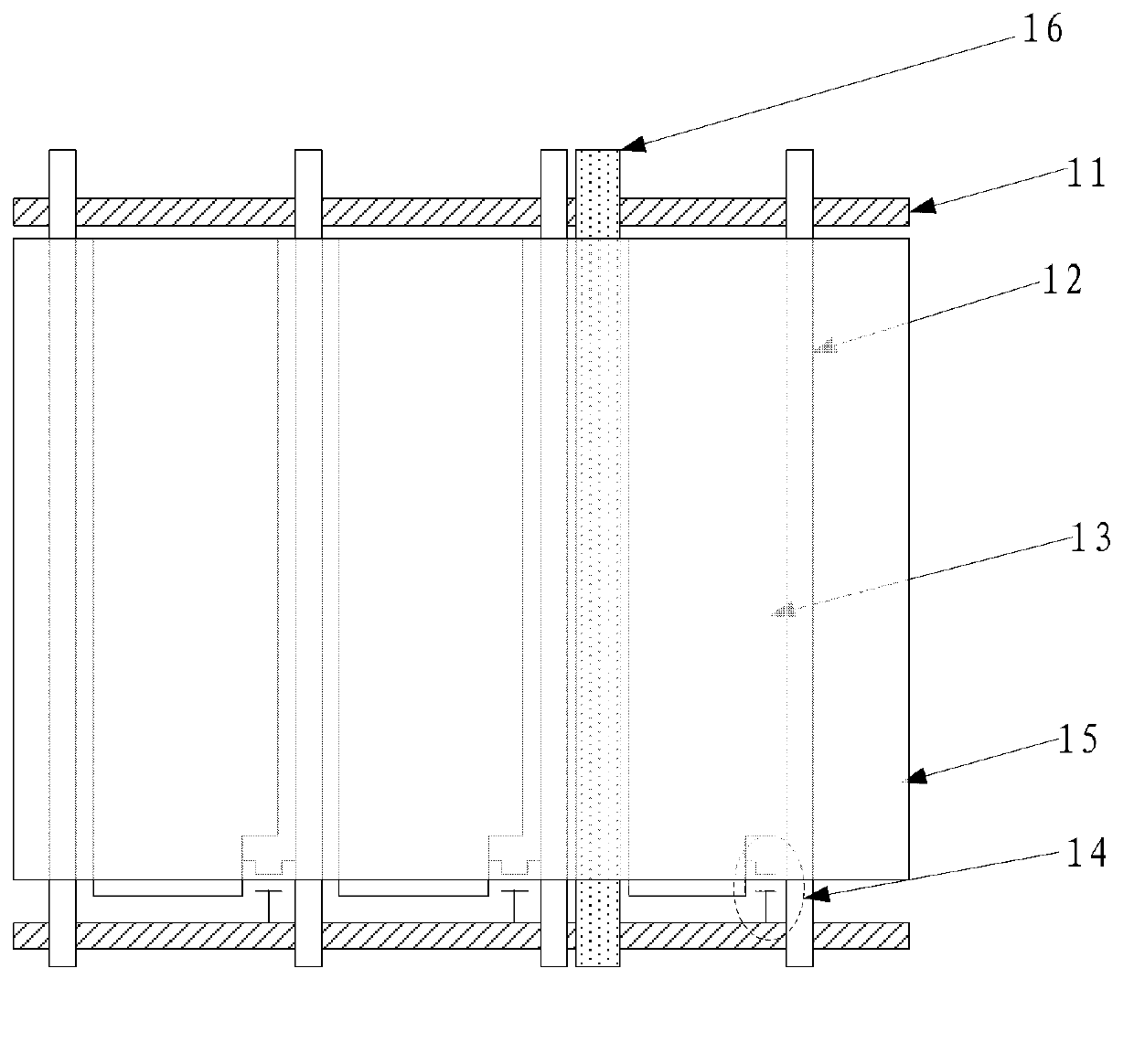
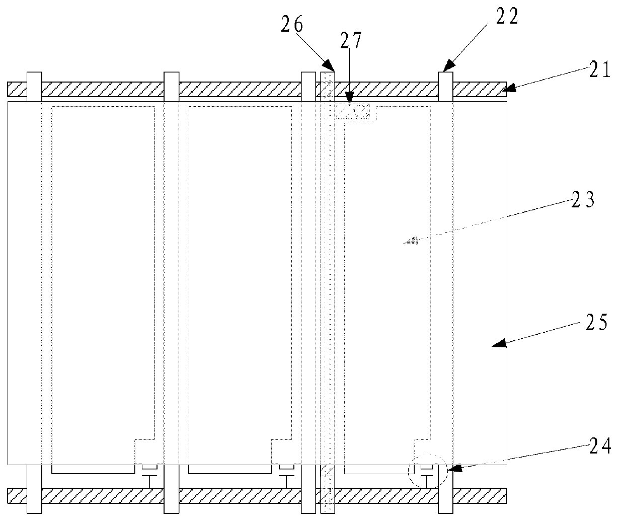
[0030] An embodiment of the present invention provides an array substrate, such as figure 2 As shown, the array substrate includes a gate line 21, a data line 22, a pixel electrode 23 and a thin film transistor 24 arranged in the pixel area defined by the gate line 21 and the data line 22, and a common electrode 25; the array substrate It also includes a first sensing line 26 and a second sensing line 27, the first sensing line 26 and the second sensing line 27 are arranged in parallel on the upper and lower layers, and are all connected to the electrode strips on the common electrode 25. Intersection arrangement; wherein, the first sensing line 26 is located betwee...


PUM


Abstract

The embodiment of the invention provides an array substrate and a manufacture method and a display device thereof and relates to the technical field of display. The aperture ratio of the display device can be improved. The touch type array substrate comprises a grid line, a data line, a pixel electrode, a thin-film transistor and a common electrode, wherein the pixel electrode and the thin-film transistor are arranged in a pixel region defined by the grid line and the data line. The array substrate further comprises a first sensing line and a second sensing line, wherein the first sensing line and the second sensing line are arranged in an upper layer and a lower layer correspondingly and parallelly, and both the first sensing line and the second sensing line are arranged in a way of crossing an electrode bar on the common electrode; and the first sensing line is arranged between a pattern layer in which the second sensing line is and a pattern layer in which the common electrode is, and the second sensing line is electrically connected with the common electrode.

Description

technical field [0001] The present invention relates to the field of display technology, in particular to an array substrate, a manufacturing method thereof, and a display device. Background technique [0002] With the development of display technology, touch display devices that integrate input and output terminals have appeared. With the advent of a series of products such as small and light hand-held touch devices, the market demand for touch display devices has surged . Among the various existing touch display devices, the projected capacitive touch device in the capacitive touch device has become the main development direction because of its advantages of real multi-touch and high sensitivity. [0003] Such as figure 1 As shown, it is an array substrate of a mutual inductive capacitive touch display device in the existing projected capacitive touch screen, and the array substrate includes gate lines 11, data lines 12, gate lines 11 and data lines 12 Pixel electrode 1...

Claims


Application Information

Patent Timeline
Patent Type & Authority Applications(China)
IPC IPC(8): H01L27/12H01L21/77G06F3/044
CPCG06F3/0445G06F2203/04103G02F1/1362G06F3/0412H01L27/124H01L27/1262
Inventor 孙建王磊薛海林陈小川
Owner BEIJING BOE OPTOELECTRONCIS TECH CO LTD
Why Eureka
Try Eureka