Micromechanical sensor arrangement, corresponding manufacturing method and application

A technology of micromechanical sensor and inertial sensor, which is applied in the direction of microstructure device, manufacturing microstructure device, processing microstructure device, etc., can solve the problem that the modular replacement of ASIC circuit chip cannot be easily realized, and achieve the elimination of geometric structure restrictions, Simplified structure technology and connection technology, low cost effect

Inactive Publication Date: 2013-09-11
ROBERT BOSCH GMBH
View PDF6 Cites 0 Cited by
  • Summary
  • Abstract
  • Description
  • Claims
  • Application Information

AI Technical Summary

Problems solved by technology

The modular replacement of ASIC circuit chips cannot be easily realized

Method used


Image

  • Micromechanical sensor arrangement, corresponding manufacturing method and application
  • Micromechanical sensor arrangement, corresponding manufacturing method and application
  • Micromechanical sensor arrangement, corresponding manufacturing method and application

Examples


Embodiment Construction

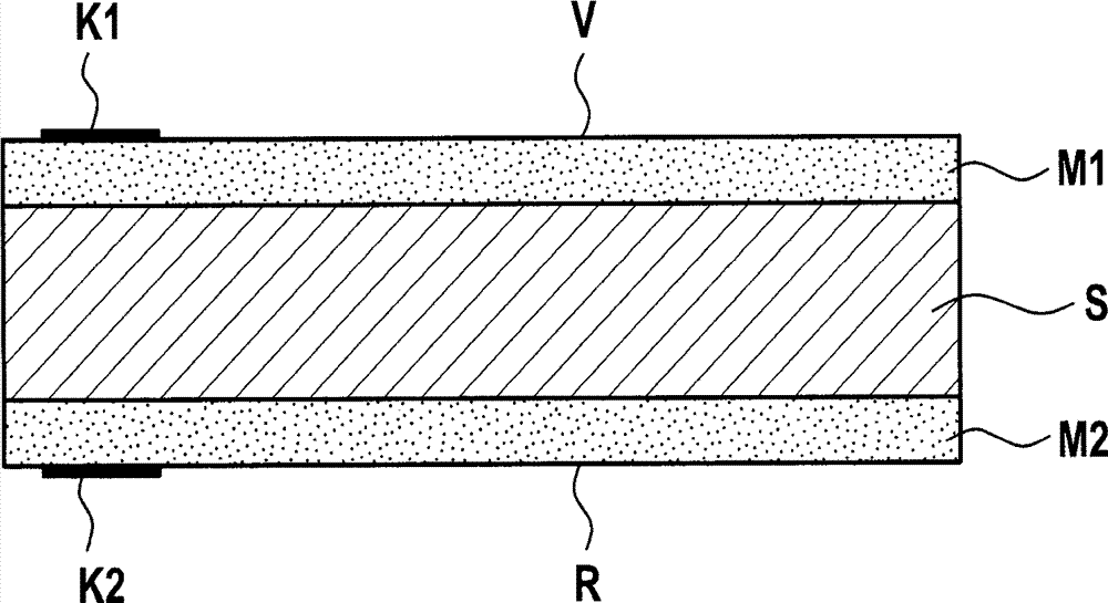
[0026] figure 1 A schematic cross-sectional view of a micromechanical sensor arrangement according to a first embodiment of the invention is shown.

[0027] exist figure 1 , the reference S designates a substrate, for example a silicon substrate, which has a front side V and a back side R. A first functional MEMS region M1 is integrated on the front side V and a second functional MEMS region M2 is integrated on the back side. A functional MEMS area is understood to mean that at least one sensor and / or actuator is built in this area. K1 designates the electrical contact area on the front side V, and K2 designates the electrical contact area on the rear side R. FIG.

[0028] Such an arrangement of the functional MEMS regions M1 , M2 on opposite sides V, R of the substrate S enables efficient integration, a small structural height and cost-effective process control.

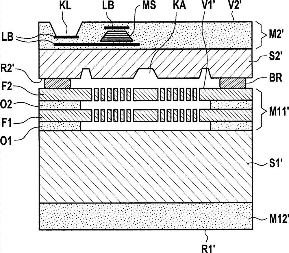
[0029] figure 2 A schematic cross-sectional view of a micromechanical sensor arrangement according to a sec...


PUM


Abstract

The invention provides a micromechanical sensor arrangement, a corresponding manufacturing method and application. The micromechanical sensor arrangement comprises substrates (S1, S1 and S') provided with front side (V, V1 and V1') and back sides (R, R1 and R1'). A first microelectromechanical sensor arrangement (M1) is integrated on the front side (V, V1 and V1') and a second microelectromechanical sensor arrangement (M2) is integrated on the back sides (R, R1 and R1').

Description

technical field [0001] The invention relates to a micromechanical sensor arrangement and a corresponding production method as well as a corresponding use. Background technique [0002] Currently, micromechanical sensor devices are manufactured either as discrete sensors on a dedicated chip or as integrated sensors together with associated evaluation circuits. In integrated sensors, there is either vertical integration, in which the sensors are arranged above the evaluation circuit, or horizontal integration, in which the sensors are arranged next to the evaluation circuit. [0003] In horizontal integration, the side-by-side mounting of the sensor chip and the ASIC analysis circuit chip requires increased lateral space and costly electrical connections must be created between the chips. In the case of vertical integration of sensor chip and ASIC evaluation circuit chip or vice versa, there are restrictions in terms of design freedom and the overall height of the structure i...

Claims


Application Information

Patent Timeline
Patent Type & Authority Applications(China)
IPC IPC(8): B81B7/00B81B7/02B81C1/00B81C3/00
CPCB81B7/02B81B2201/025
Inventor G.比肖平克C.舍林
Owner ROBERT BOSCH GMBH
Why Eureka
Try Eureka