A dsp debugging device

A test system and address technology, applied in software testing/debugging, instrumentation, electrical digital data processing, etc., can solve problems such as system difficulties, occupation of bus resources, and many pins

Inactive Publication Date: 2016-01-13
SHANGHAI JIAOTONG UNIV +1
View PDF3 Cites 0 Cited by
  • Summary
  • Abstract
  • Description
  • Claims
  • Application Information

AI Technical Summary

Problems solved by technology

But the JTAG debugging device has the following deficiencies: 1. The JTAG interface uses a serial method to transmit data, and the devices on the JTAG chain share the communication bandwidth. When there are many devices mounted, the debugging communication rate will be severely reduced.
2. JTAG cannot read and write a large amount of data to the DSP system, and the debugging efficiency is low
3. Limited by the JTAG hardware interface, the real-time performance of debugging is not strong
4. The number of DSPs connected in series on the JTAG chain is limited, and the number of DSPs supported by the JTAG debugging device at the same time is limited, so it is difficult to debug a system with multiple DSPs in parallel
However, if the SoC directly adopts the AHB interface, too many pins are required, even if only considering the AHB clock, address bus (32bits), data bus (32bits), etc., there are already more than 60, occupying a lot of bus resources

Method used


Image

  • A dsp debugging device
  • A dsp debugging device
  • A dsp debugging device

Examples


Embodiment Construction

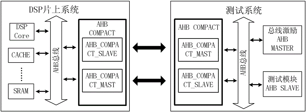
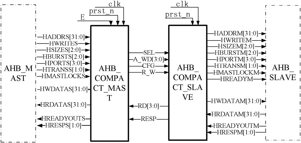
[0075] A kind of DSP debugging device provided by the invention (such as figure 1 The AHB_COMPACT module shown in ) mainly includes two submodules AHB_COMPACT_MAST and AHB_COMPACT_SLAVE, respectively having an AHB interface and an AHB_COMPACT interface, and the position of the DSP debugging device in the DSP debugging system is as follows figure 1 shown. The IP modules in the DSP system-on-chip are interconnected through the AHB on-chip bus, and the AHB_COMPACT module is mounted on the AHB bus as an IP module, and communicates with the off-chip debugging system through the simplified AHB_COMPACT interface. The off-chip test system also needs to include the AHB_COMPACT module to convert the AHB_COMPACT interface signal into an AHB interface signal in reverse. Therefore, the bus excitation module AHBMSATER in the test system can input the excitation signal to the DSP system on chip through the AHB_COMPACT_SLAVE interface of the DSP system on chip, or read the data that needs to...


PUM


Abstract

The invention provides a DSP (Digital Signal Processor) debugging device which comprises two submodules of AHB_COMPACT_MAST and AHB_COMPACT_SLAVE. The device, serving as an independent IP (Internet Protocol) module, is in cascade connection with an on-chip AHB (Advanced High performance Bus) bus, and communicates with out-chip equipment through an AHB_COMPACT interface; and meanwhile, the device, serving as a part of an out-chip debugging unit, completes conversion from the AHB_COMPACT interface to an AHB interface. The AHB_COMPACT_MAST module is connected with the MAST interface of the on-chip AHB bus, and the MAST interface is converted into the AHB_COMPACT interface to be connected with a below-chip test module. The AHB_COMPACT_SLAVE is connected with an SLAVE interface of the on-chip AHB bus, and the SLAVE interface is converted into an AHB_COMPACT interface to be connected with the below-chip test module. According to the DSP debugging device, the data transmission of the two modules is completed under different AHB transmission modes through two state machines of AHB_COMPACT_MAST_FSM and AHB_COMPACT_SLAVE_FSM. A below-chip debugging unit is used for performing conversion of signals from the AHB_COMPACT interface to the AHB interface just by using the device as well in an out-chip system so as to complete communication between a DSP on-chip system and out-chip AHB equipment. The DSP debugging device provided by the invention is more flexible, more efficient, better in real time and larger in throughput, and simultaneously bus resources are also greatly saved.

Description

technical field [0001] The invention relates to a DSP debugging device, in particular to a debugging device with an AHB interface, which utilizes a small amount of bus resources to complete data reading and writing for a DSP on-chip system. Background technique [0002] Usually the hardware debugger is the main tool for debugging DSP. At present, most DSPs and their corresponding hardware debuggers have JTAG (JointTestActionGroup) debugging interface, that is, standard test access interface and boundary scan structure. But the JTAG debugging device has the following deficiencies: 1. The JTAG interface transmits data in a serial manner, and the devices on the JTAG chain share the communication bandwidth. When there are many mounted devices, the debugging communication rate will seriously drop. 2. JTAG cannot read and write a large amount of data to the DSP system, and the debugging efficiency is low. 3. Limited by the JTAG hardware interface, the real-time performance of de...

Claims


Application Information

Patent Timeline
Patent Type & Authority Patents(China)
IPC IPC(8): G06F11/36G06F13/40
Inventor 周鸿斌孔吉刘佩林
Owner SHANGHAI JIAOTONG UNIV
Why Eureka
Try Eureka